RS232 signals cover a much longer distance than standard TTL and I2C signals. Also, RS232 signals have better noise immunity. RS232 is a well-known standard supported by many popular integrated circuits (ICs) and therefore is still widely used. Sometimes we want to send TTL and I2C signals over a longer distance. This article describes how these signals can be extended through RS232 lines.
Circuit and working
Fig. 1 shows the circuit of configurable RS232 to TTL to I2C adaptor. RS232 signals are available on the standard 9-pin connector, also known as DB9 connector (CON1). There is a wide variety of configurations available for RS232 signals on different peripherals. So we have provided CON2 and a 4-way or 8-pin DIP switch (DIP1) for various configurations. CON2 is a single-line connector from which RS232 signals can be taken for interfacing external circuits.
Fig. 1 Circuit of configurable RS232 to TTL to I2C adaptor
MAX232 (IC1) is a dual driver/receiver that includes a capacitive voltage generator to supply TIA/EIA-232-F voltage levels from a single 5V supply. It has two receivers and two transmitters compatible with RS232 signals.
TTL equivalent signals from the interface are available at CON3. These signals drive LED1 through LED4 through gates N1, N4, N5 and N6 of hex inverter 7405 (IC2) for visual indications. The 7405 should be with low input current and capable of driving the LEDs.
Switches S1 and S2 are used to manually check the signals on LED1 and LED2 when DIP2 pins 1 and 8 and pins 3 and 6 are shorted. DIP2 is used to provide different configurations for TTL to I2C converter built around inverters N2 and N3 of IC2. I2C signals are available on CON5.
Vs+ and Vs– at pins 2 and 6 respectively of IC1 are the two test points where the voltage levels obtained should be around 9V. These voltages are produced internally by MAX232 and should be within specified limits as stated in the data sheet.
The circuit requires a 5V DC regulated power supply and below 100mA of current to operate. You may use a small transformer providing around 10V/100mA and a 7805 regulator for the power supply. Regulator IC should be mounted on a heat-sink having thermal resistance below 30oC/W.
You can provide two appropriate connectors at the power supply output: one for the adaptor circuit and another for the digital or embedded circuit for interfacing TTL or I2C signals.
Fig. 2 Actual-size PCB pattern of configurable RS232 to TTL to I2C adaptorFig. 3 Component layout of the PCB
Construction and testing
An actual-size, single-side PCB pattern of configurable RS232 to TTL to I2C adaptor circuit is shown in Fig. 2 and its component layout in Fig. 3. After mounting all components on the PCB, check proper connections again in the circuit. Connect the 5V DC power supply source to CON4 to power on the circuit.
Next, connect connector DB9 to the computer and send digital signals from serial communication software (for example, HyperTerminal) to the circuit. If none of the LEDs glow, check proper connections on DIP1 and DIP2 and ensure that transmit (pin 3) and receive (pin 2) pins of DB9 are connected to the appropriate pins. Otherwise, toggle S1 and S2; LED1 and LED2 should glow, respectively.
If everything is working fine, you may transmit any digital signals, either TTL or I2C or RS232, from DB9 to CON3 and CON5.
Petre Tzv Petrov was a researcher and assistant professor in Technical University of Sofia (Bulgaria) and expert-lecturer in OFPPT(Casablance), Kingdom of Morocco. Now he is working as an electronics engineer in the private sector in Bulgaria
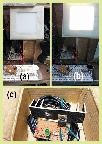
Despite being more expensive than standard permanent outdoor toilets, portable toilets (Fig. 1) have several significant benefits as these are self-contained and can be placed almost anywhere. These days portable toilets are frequently seen at outdoor areas like construction sites, farms, camp sites and even street-sides. Solar power provides an ideal solution for applications where lighting is required in portable toilets that are located away from a mains supply grid, or the installation is expected to be on the site for a brief period.
Here is a circuit of a self-contained solar light for portable toilet lighting applications. The solar light housed within its own enclosure comprises a solar charger, rechargeable battery pack, white LED light source and PIR motion sensor as an occupancy sensor. The occupancy sensor (motion sensor) activates the light source and, after the booth has been vacated (or when there is no valid motion), the lighting switches off to save battery.
Circuit and working
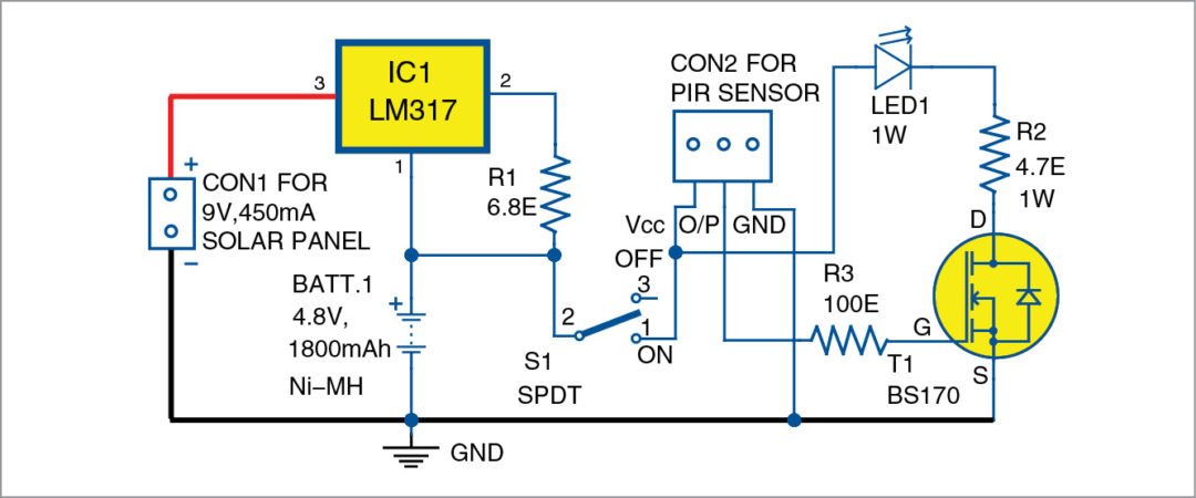
Circuit diagram of the solar light for a portable toilet is shown in Fig. 2. It is built around a 9V, 450mA solar panel, voltage regulator LM317 (IC1), a PIR sensor, MOSFET BS170 (T1), a 1W white LED (LED1) and a few other components.
Fig. 2: Circuit diagram of the solar light for a portable toilet
The circuit may be split into two sections: the charger and the sensing and control system. Power is supplied via the 9V, 450mA-rated polycrystalline solar panel, which is linked to CON1 and charges the 4.8V, 1800mAh battery pack, BATT.1, via the constant-current charger built around IC1. The 6.8-ohm resistor (R1) limits the charging current to near one-tenth rate of the battery, that is, 180mA.
The sensing and control circuitry is based on PIR motion detector module (Fig. 3), which is connected across CON2. When a valid motion is detected, output of the PIR sensor goes to around 3.3V and the light source LED1 (3.6V, 1W white LED) is switched on through medium-power MOSFET BS170 for a finite time. The 4.7-ohm, 1W resistor R2 limits the operating current of the white LED.
Fig. 3: Photo of the PIR sensor
Construction and testing
An actual-size, single-side PCB for the solar light for a portable toilet is shown in Fig. 4 and its component layout in Fig. 5. Enclose the PCB in a suitable small box in such a way that it can be fitted in the toilet.
Fig. 4: Actual-size PCB of the solar light for a portable toiletFig. 5: Component layout of the PCB
After assembling the PCB board, connect the fully-charged battery pack BATT.1 to the circuit and switch on S1. The PIR motion sensor detector requires an initialisation time of about 60 seconds (or even up to three minutes). Thereafter, it enters standby mode, ready for detection.
You can adjust the delay potmeter in PIR sensor clockwise to increase the time delay from three seconds to up to 300 seconds. Similarly, turning the sensitivity pot in PIR sensor clockwise increases the detection sensitivity from three to six metres. In some PIR sensor potmeters, the LDR socket option is not provided.
The solar panel (not fitted within the enclosure) can be mounted at an appropriate location. Battery pack BATT.1 is best linked to the circuit via two flexible, well-insulated multi-strand wires. Then, a heat-sink should be added to IC LM317.
Finally, house the assembled PCB in a small plastic case with holes drilled for the connectors for linking the solar panel, switch S1, LED1 and PIR motion sensor. The suggested enclosure is shown in Fig. 6.
Fig. 6: Suggested enclosure
EFY note. Connect LED1 externally, with a proper heat-sink, to CON3 in the PCB.
T.K. Hareendran is an electronics hobbyist, freelance technical writer and circuit designer
Fig. 1: Author’s prototype: (a) dawn mode, (b) dusk mode and (c) prototype
Solar streetlights can be easily integrated with a dusk-dawn controller by simply employing a pnp transistor and a few resistors where the solar panel itself works as the sensor. But what about other lighting sources that do not employ solar panels such as automatic lighting systems in small wind turbines, automatic lighting in cars or battery based systems where automatic lighting is necessary?
A simple, low-cost, yet an effective solution for the dusk-dawn controller circuit is described here. Author’s prototype is shown in Fig. 1.
Circuit and working
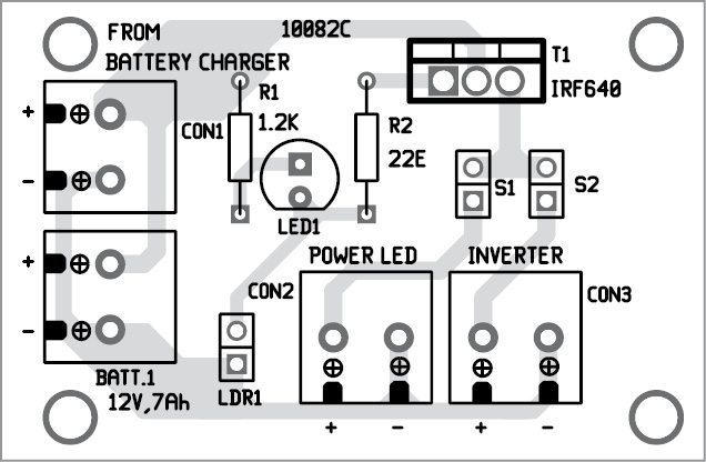
Circuit diagram of the dusk-dawn controller is shown in Fig. 2. It is built around a light-dependent resistor (LDR1), n-channel MOSFET IRF640 (T1), 12V LED light or a small inverter (100W) and a few other components.
The 12V battery-operated circuit is designed such that the common battery supply is used for operating the circuit as well as for load, that is, for power LED/small inverter circuit. Resistors R1 and R2 are used as a voltage divider and a current limiter in the circuit, respectively. LED1 is used as circuit de-activation indicator. LDR1 is the main component for actuation of the dusk-to-dawn sensing. The n-channel MOSFET IRF640 is for the switching action of the LED light or the small inverter connected to the system through switches S1 and S2, respectively.
With daylight falling on LDR1 (dawn mode), resistance of LDR1 becomes low, a small current flows through LED1 and it glows. At the same time, due to low voltage across LDR1, MOSFET IRF640 does not trigger. So load (LED light/inverter) remains off.
But when the surrounding area of LDR1 (dusk mode) is dark (at night), resistance of LDR1 becomes very high, no current flows through LED1 and it does not glow. At the same time, due to higher voltage across LDR1, IRF640 triggers. So load light (power LED light/ inverter) comes on, provided switch S1 or S2 is on.
IRF640 can handle a maximum current of approximately 18A, but you can limit its application to approximately 8A-9A only, based on which the heat-sink is attached to the MOSFET.
Fig. 2: Circuit diagram of the dusk-dawn controller
Construction and testing
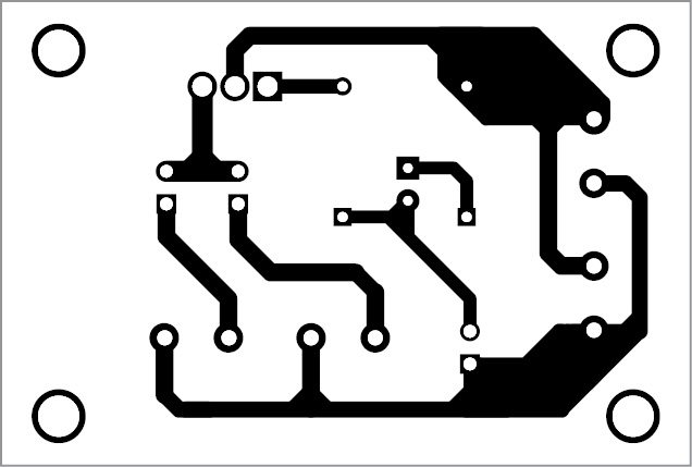
An actual-size, single-side PCB for the dusk-dawn controller is shown in Fig. 3 and its component layout in Fig. 4.
Fig. 3: Actual-size PCB pattern of the dusk-dawn controllerFig. 4: Component layout of the PCB
After assembling the circuit, enclose it in a suitable box. The unit should be fixed on the pillar in such a way that the daylight falls directly on LDR1.
Bikash Rai is assistant engineer in Energy & Power Department, government of Sikkim. He is also a part-time research scholar at Sikkim Manipal Institute of Technology, Sikkim
The circuit for an LPG leakage detector is readily available in the market, but it is extremely expensive and usually based on a microcontroller (MCU). Presented here is a low-cost circuit for an LPG detector that you can build easily.
The main objective of the circuit is to detect LPG leakage anywhere. Fig. 1 shows the author’s prototype.
Fig. 1: Author’s prototypeFig. 2: Circuit diagram of the LPG detector
Circuit and Working
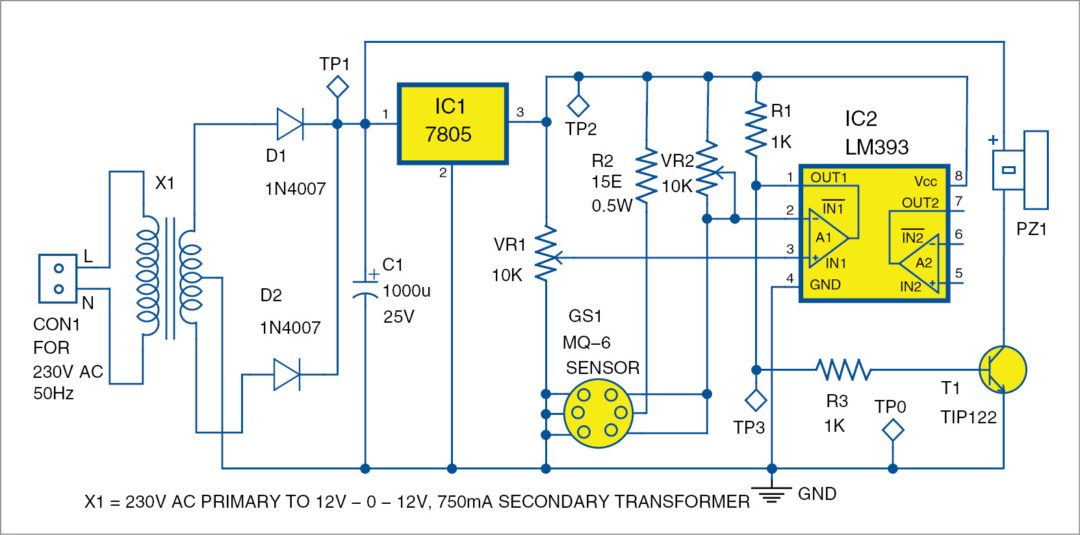
Circuit diagram of the low-cost LPG detector is shown in Fig. 2. It is built around step-down transformer X1, two rectifier diodes 1N4007 (D1 and D2), a 1000µF capacitor (C1), 7805 voltage regulator (IC1), MQ-6 LPG gas sensor (GS1), dual comparator LM393 (IC2), darlington transistor TIP122 (T2), 12V high-gain siren/buzzer (PZ1) and a few other components.
The mains supply is stepped down by transformer X1, rectified by a full-wave rectifier comprising diodes D1 and D2, filtered by capacitor C1 and fed to regulator 7805 (IC1) to maintain constant 5V DC output, which is fed to the circuit.
At the heart of the circuit is dual comparator IC LM393 (IC2). It is used to compare two different voltages, namely, reference voltage and MQ-6 gas sensor output voltage.
Reference voltage at non-inverting pin 3 of IC2 is set using potmeter VR1 to adjust voltage levels based on sensitivity requirements. LPG sensor (MQ-6) output voltage is fed to inverting pin 2 of IC2.
If reference voltage (pin 3 of IC2) is less than sensor voltage (pin 2 of IC2), output goes low, which means there is no LPG leakage. With low output, T1 remains cut-off and there is no current flow through the buzzer; it does not sound and remains in silence mode.
If reference voltage is greater than sensor voltage, output goes high, which means there is LPG leakage. The high output switches on transistor T1 and the buzzer rings loudly to alert the people around.
It is very easy to find gas leakages with this circuit, which uses low-cost components and an interactive way to adjust different sensitivity levels, based on customer needs, with the help of potmeter VR1.
Construction and testing
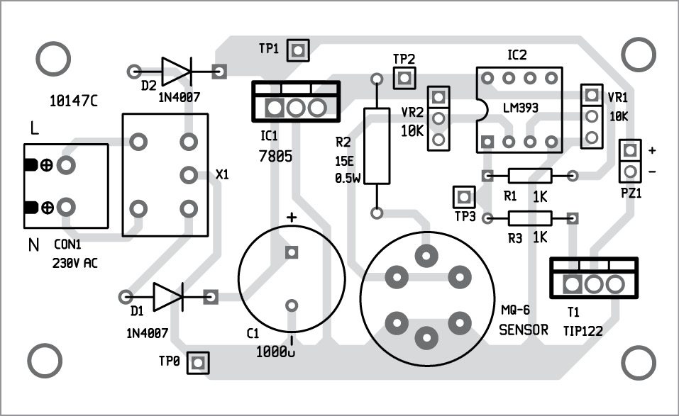
An actual-size PCB pattern of the LPG detector is shown in Fig. 3 and its component layout in Fig. 4.
Fig. 3: Actual-size PCB pattern of the LPG detectorFig. 4: Component layout of the PCB
After assembling the circuit on a PCB, enclose it in a box with an opening for the gas to enter. Place the unit near the LPG cylinder or gas stove, within a distance of one metre. Vary preset VR1 to adjust sensitivity of the sensor.
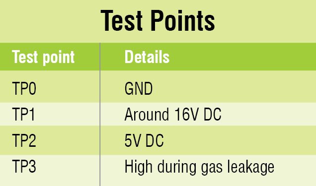
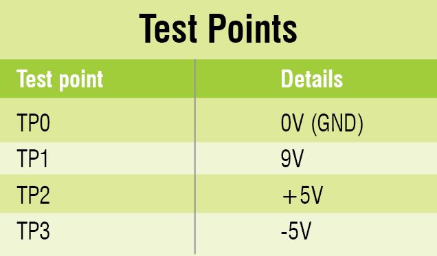
Verify the voltages are as per test points table before using the circuit. Now, spray the gas from the bottle (as shown on the left side of author’s prototype) towards MQ-6 gas sensor and measure voltage at TP3; it should be high.
If you do not have a gas-filled bottle, place the unit near the gas stove burner and turn it on for a few seconds without igniting. Then, turn the burner off and adjust VR1 until buzzer sounds.
Pamarthi Kanakaraja is associate professor (R&D cell) in Usharama College of Engineering and Technology, Andhra Pradesh. He has been working in the field of embedded designing and programming concepts for the last six years
A thermostat is a standard equipment for sensing temperature of a system and maintaining it at a pre-defined point. It is a regular feature in air-conditioners, room heaters and refrigerators. Although some commercially-available refrigerators have inbuilt thermostats, the given circuit is easy to build and automatically turns on or turns off the appliance at pre-set temperatures.
My refrigerator’s deep freezer’s temperature remains between -5°C to -15°C (former temperature switches the fridge on and the latter turns it off).
Circuit and working
The 230V AC mains voltage instead of going directly to the refrigerator (or input of the automatic voltage stabiliser, if used with the fridge) is routed through the normally open (N/O) contact of relay RL1. When the relay gets energised due to conduction of T2 (BC547), relay contact is closed and the appliance gets 230V AC power, which, in turn, starts cooling.
Fig. 1: Circuit of the electronic thermostat for a fridge
IC1 is a quad comparator (LM339) used as a voltage comparator with hysteresis. Inverting input of IC1 is applied to a reference voltage derived from Zener diode ZD1 (5.2V), which is then further divided by the potential divider arrangement provided by R3, R5 and VR1. C5 is the decoupling capacitor to bypass AC noise, if any.
Heart of the circuit. Between the non-inverting input of IC1 and the ground is the temperature sensor, which is an npn silicon transistor 2N2222 with its collector shorted to its base. The transistor’s temperature-dependent characteristic of the base-emitter junction is used as the temperature-sensing property. For every degree rise, junction voltage decreases by 2mV. Trimpot VR1 is adjusted to the reference voltage at a value equal to the sensor’s junction voltage corresponding to the lower negative temperature (-5°C in this case).
On state. If temperature inside the fridge is between -5°C and -15°C, then voltage at the inverting input of the comparator is equal to reference voltage (corresponding to voltage for -5°C) plus fraction of the voltage feedback through potential dividers R7 and R4. Feedback voltage in this case is 20mV corresponding to a temperature change of 10°C. Thus, as long as temperature is more than -15°C, voltage at inverting input is greater than that at non-inverting input, comparator output pin 2 is high, T2 is saturated and energises the relay coil and the appliance remains switched on.
Off state. When temperature goes below -15°C, comparator output goes low, relay gets de-energised and the appliance goes into off state. When comparator goes low, feedback voltage of 20mV vanishes and voltage at the inverting input corresponds to a temperature of -5°C. So the temperature cycles between -5°C and -15°C.
Reference setting using VR1 decides the less negative of the two temperature extremes and the hysteresis depends on the voltage divider arrangement of R7 and R4.
Let ‘T’ be the desired temperature hysteresis, then,
T (°C)=(3000×R4)/(R4+R7)
Power supply. DC supply for the circuit including the relay consists of a conventional bridge rectifier, step-down transformer X1 and filter capacitor C1, along with 3-terminal voltage regulator 7812. C2 is a decoupling capacitor commonly used at the output of the voltage regulator.
Construction and testing
An actual-size PCB layout of the electronic thermostat circuit for a fridge is shown Fig. 2 and its component layout in Fig. 3.
Fig. 2: Actual-size PCB layout of the electronic thermostat circuitFig. 3: Component layout of the PCB
Sensor transistor 2N2222 should be mounted on the side wall of the freezer with some epoxy (like Araldite). Connections from the sensor to the circuit should be made with a shielded cable made of materials like polycab coatings. Leads should be fully insulated from each other and from the transistor body using some epoxy so that water deposition on the sensor does not short these.
I housed the sensor’s metallic body in a ceramic block and affixed it to the freezer’s body. This fitting is quite tight to ensure complete thermal contact. Ceramic is the best thermal conductor and electrical insulator.
Calibration is done by bringing the sensor in contact with ice water and at the same time biasing its base emitter junction at about 100µA using a series resistance and suitable voltage. Junction voltage thus observed corresponds to 0°C. Junction voltage corresponding to any other temperature can then be determined from the figure of temperature coefficient (-5mV/°C).
For troubleshooting, ensure various test points are as per the voltages listed in the test point table.
Sundar B. is M.Sc. Physics (electronics). Currently, he is working as senior technical associate at Institute of Chemical Technology, Mumbai
This circuit is designed for use with all kinds of medium-power automobile/domestic 12V DC loads. It is a simple solid-state relay (SSR) switch, controlled by a standard passive infrared (PIR) motion sensor module. A PIR sensor is an electronic device that can measure IR light radiating from objects in its field-of-view.
Apparent motion is detected when an IR source with one temperature (such as a human being) passes in front of an IR source with another temperature (such as a wall). The PIR sensor module, centred on a PIR sensor, has elements made of crystalline material that generates an electric charge when exposed to IR radiation.
Fig. 1: PIR motion sensor module and its dome shaped cover (inset)Fig. 2: PIR motion Sensing SSR Switch
Changes in the amount of IR striking the element change the voltages generated, which are measured by an onboard circuitry. The module contains a special filter called Fresnel lens, which focuses IR signals onto the sensor element. As ambient IR signals change rapidly, onboard circuitry triggers the output to indicate motion. Fig. 1 shows the PIR motion sensor module. It is usually hidden behind a translucent dome shaped cover as shown in the inset in Fig. 1.
Circuit and working
Circuit diagram of the PIR motion-sensing SSR switch is shown in Fig. 2. It is built around a PIR motion-sensor module (connected across CON2), MOSFETs BS170 (T1) and IRF9540 (T2), rectifier diode 1N4007 (D1) and a few other components.
The PIR sensor module has a 3-pin connection for Vcc, output and ground, and provides a single output that goes high when motion is detected. It also has a 2-pin jumper selection for single or continuous trigger output mode. The two positions are labelled H and L (Fig. 1).
When the jumper is at H position, output goes high whenever the sensor is triggered and retriggered. In position L, output goes high and low like a monostable timer every time the sensor is triggered. Retriggering pulse does not affect the output duration.
The circuit presented here is in repeatable trigger mode and turns T2 on when sensor output goes high. Output of the PIR sensor module is connected to the base of T1 (BS170) via resistor R1.
When motion is detected, PIR sensor output goes high to about 3.3V. The high-level, standard TTL output from the sensor-module switches on MOSFET T2 through T1, and T2 is closed by this action. As a result, the connected DC load is powered through T2 for a finite duration, determined by the time-delay setting of the PIR sensor module. Usually, the PIR sensor module includes an onboard time control preset pot (Fig. 1), which is adjustable from seconds to minutes. LED1 is the power-on indicator.
Fig. 3: Actual-size PCB pattern of the PIR motion-sensing SSR switchFig. 4: Component layout of PCB
Construction and testing
An actual-size, single-side PCB for the PIR motion-sensing SSR switch is shown in Fig. 3 and its component layout in Fig. 4. Enclose the PCB in a small box so that you can connect 12V IN and 12V OUT easily at the rear side of the box. Install the PIR sensor at a suitable place and connect it to the PCB using a three-wire cable.
EFY notes.
1. During initial power-up, the circuit automatically switches to active mode for a while and then shifts back to sleep mode.
2. p-channel power MOSFET IRF 9540 (in TO-220 package) is preferred universally for all commercial/industrial applications at power dissipation levels up to approximately 50 watts.
3. According to the data sheet, the PIR sensor requires an initial stabilisation time of 10 to 60 seconds in order to function properly. During this time, any motion in its field-of-view (approx. 6 metres) should be avoided.
T.K. Hareendran is an electronics hobbyist, freelance technical writer and circuit designer
Presented here is a red, green and blue (RGB) colour generator using AT89C2051 microcontroller (MCU). This is a simple and low-cost circuit for a multiple colour generator that can be built easily with a few additional components. The main objective of the project is to generate multiple colours from RGB primary colours as used in television displays, computer monitors and other colour displays for commercial applications like LED projectors. The concept of primary colour mixing is shown in Fig. 1.
Additive mixing of red and green lights produces shades of yellow, orange or brown. Mixing green and blue produces shades of cyan, whereas mixing red and blue produces shades of purple including magenta. Mixing nominally equal proportions of the three primaries results in shades of grey or white; colour space that is generated is called an RGB colour space.
Circuit and working
The circuit diagram for the multiple colour generator is shown in Fig. 2. The circuit requires a 9V battery, 7805 voltage regulator (IC1), Atmel AT89C2051 MCU (IC2) and a few other components. The 20-pin MCU performs the operation of multiple colour generation from RGB primary colours on pressing switches S1 through S4. In this project, we have used the concept of pulse width modulation (PWM) to change the colours of the RGB LED.
Fig. 2: Circuit of the RGB colour generator
Initially, the circuit is powered by a +9V supply, which is connected to IC1 to maintain a constant +5V at its output. This constant output is fed to the MCU circuit. Port3 of IC2 is used to drive common-anode RGB LED, with P3.0 connected to red pin, P3.1 to green pin and P3.2 to blue pin of the RGB LED. Port1 is connected to the four tactile switches S1 through S4 for producing multiple colours.
When the circuit is switched on, red colour of the RGB LED glows for a preprogrammed time interval of three seconds. It then switches off for three seconds. This is followed by green and blue colours switching on and off in a similar manner and for the same time periods.
Now, when we press switch S1, we get yellow colour (red+green), and if we press switch S2, we get magenta (red+blue). If we press switch S3, we get cyan (blue+green), and if we press switch S4, we get multiple colours with the help of PWM technique.
Software
The software is written in embedded C language and compiled using Keilµvision 4 version compiler. It contains simple switch statements to produce different colours from primary colours. We have used Topwin 6 software to burn the hex code into the MCU using a Universal Topwin programmer board.
Construction and testing
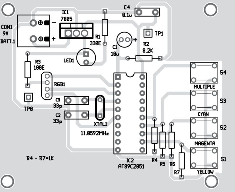
An actual-size, single-side PCB of the circuit is shown in Fig. 3 and its component layout in Fig. 4. Assemble the circuit on the PCB as it minimises time and assembly errors. Carefully assemble the components and double-check for any error(s). Use a proper IC base for the MCU.
Fig. 3: Actual-size PCB pattern of the RGB colour generatorFig. 4: Component layout of the PCB
CON1 is a 2-pin connector used to connect a 9V battery.
For troubleshooting, verify the voltages listed in the test points table.
Pamarthi Kanakaraja is associate professor (R&D cell) at Usha Rama College of Engineering and Technology, Telaprolu, Andhra Pradesh. He has been working in the field of embedded designing and programming concepts for the last six years
Op-amps require dual-polarity supply for proper operation. When working with battery supply, it becomes difficult to get dual power supply for the op-amps. Presented here is a simple circuit that provides ±5V from a 9V battery.
Fig. 1: Circuit diagram of ±5V supply from 9V battery
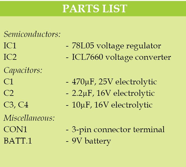
Circuit and working The circuit diagram for the ±5V supply from a 9V battery is shown in Fig. 1. It is built around 9V battery (BATT.1), voltage regulator IC 78L05 (IC1), CMOS voltage converter ICL7660 (IC2) and a few other components.
Voltage regulator IC1 converts 9V battery input into regulated 5V. This 5V output from IC1 is given to pin 8 of IC2. IC2 and capacitors C3 and C4 form the voltage inverter section that converts +5V to -5V. Converted -5V supply is available at pin 5 of IC2. Converted ±5V supply is thus available at connector CON1.
Construction and testing
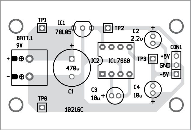
Fig. 2: Actual-size PCB layout of ±5V supply from 9V batteryFig. 3: Component layout of the PCB
An actual-size, single-side PCB for±5V supply from 9V battery is shown in Fig. 2 and its component layout in Fig. 3.
Assemble the circuit on the PCB and enclose it in a water-proof box. Battery BATT.1 should be enclosed in the box. Fix CON1 on the front or rear side of the cabinet, so that you can use the ±5V easily.
Before using the circuit, verify the test points given in the table to ensure proper working of the circuit.
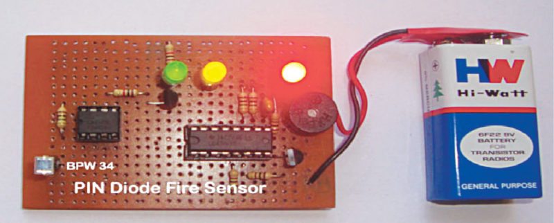
Here is an ultra-sensitive fire sensor that activates an alarm when it detects fire. Thermistor based fire alarms have a drawback; the alarm turns on only if the fire heats the thermistor in close vicinity. In this circuit, a sensitive PIN diode is used as a fire sensor for a longer-range fire detection.
Fig. 1: Author’s prototype
It detects visible light and infrared (IR) in the range of 430nm – 1100nm. So visible light and IR from the fire can easily activate the sensor to trigger the alarm. It also detects sparks in the mains wiring and, if these persist, it gives a warning alarm.
It is an ideal protective device for showrooms, lockers, record rooms and so on. Author’s prototype is shown in Fig. 1.
PIN diode BPW34 (Fig. 2) is used in the circuit as light and IR sensor. BPW34 is a 2-pin photodiode with anode (A) and cathode (K). The anode end can easily be identified from the top-view flat surface of the photodiode. A small solder point to which a thin wire is connected is the anode and the other one is the cathode terminal.
Fig. 2: BPW34 PIN photodiode
BPW34 is a tiny PIN photodiode or mini solar cell with radiant sensitive surface that generates 350mV DC open-circuit voltage when exposed to 900nm light. It is sensitive to natural sunlight and also to light from fire. So it is ideal for use as a light sensor.
BPW34 photodiode can be used in zero-bias as well as reverse-bias states. Its resistance decreases when light falls on it.
Circuit and working
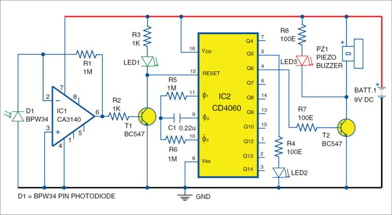
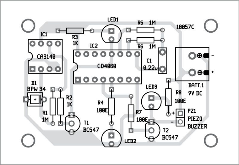
Circuit diagram of the PIN diode based fire sensor is shown in Fig. 3. It is built around 9V battery, PIN diode BPW34 (D1), op-amp CA3140 (IC1), counter CD4060 (IC2), transistors BC547 (T1 and T2), a piezo buzzer (PZ1) and a few other components.
Fig. 3: Circuit diagram of the PIN diode based fire sensor
In the circuit, PIN photodiode BPW34 is connected to the inverting and non-inverting inputs of op-amp IC1 in reverse-biased mode to feed photo current into the input of op-amp. CA3140 is a 4.5MHz BiMOs op-amp with MOSFET inputs and bipolar output.
Gate-protected MOSFET (PMOS) transistors in the input circuit provide very high input impedance, typically around 1.5T ohms. The IC requires very low input current, as low as 10pA, to change output status to high or low.
In the circuit, IC1 is used as a transimpedance amplifier to act as a current-to-voltage converter. IC1 amplifies and converts the photo current generated in the PIN diode to the corresponding voltage in its output. The non-inverting input is connected to the ground and anode of photodiode, while the inverting input gets photo current from the PIN diode.
Large-value feedback resistor R1 sets the gain of the transimpedance amplifier since it is in inverting configuration. Connection of non-inverting input to ground provides low impedance load for the photodiode, which keeps the photodiode voltage low.
The photodiode operates in the photovoltaic mode with no external bias. Feedback of the op-amp keeps the photodiode current equal to the feedback current through R1. So the input offset voltage due to the photodiode is very low in this self-biased photovoltaic mode. This permits a large gain without any large-output offset voltage. This configuration is selected to get large gain in low-light conditions.
Normally, in ambient light condition, photocurrent from the PIN diode is very low; it keeps output of IC1 low. When the PIN diode detects visible light or IR from fire, its photo current increases and transimpedance amplifier IC1 converts this current to corresponding output voltage. High output from IC1 activates transistor T1 and LED1 glows. This indicates that the circuit has detected fire. When T1 conducts, it takes reset pin 12 of IC2 to ground potential and CD4060 starts oscillating.
IC2 is a binary counter with ten outputs that turn high one by one when it oscillates due to C1 and R6. Oscillation of IC2 is indicated by the blinking of LED2. When output Q6 (pin 4) of IC2 turns high after 15 seconds, T2 conducts and activates piezo buzzer PZ1, and LED3 also glows. The alarm repeats again after 15 seconds if fire persists.
You can also turn on an AC alarm that produces a loud sound by replacing PZ1 with a relay circuitry (not shown here). The AC alarm is activated through contacts of the relay used for this purpose.
Construction and testing
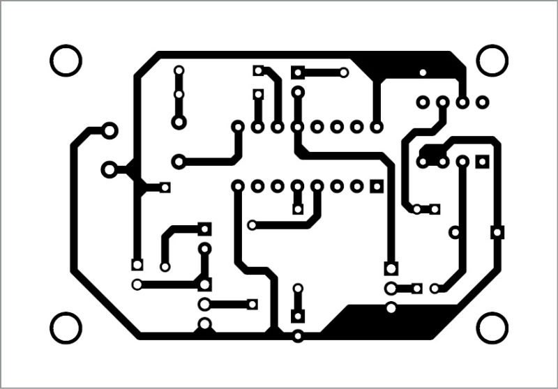
An actual-size, single-side PCB for the PIN diode based fire sensor is shown in Fig. 4 and its component layout in Fig. 5. Enclose the PCB in a small box in such a way that you can connect PIN diode BPW34 easily at the rear side of the box. Install the PIN diode in a suitable place and cover it such that normal light/sunlight does not fall on it.
Fig. 4: PCB layout of the PIN diode fire alarmFig. 5: Component layout of the PCB
Testing the circuit is simple. Normally, when there is no fire flame near the PIN diode, the piezo buzzer does not sound. When a fire flame is sensed by the PIN diode, piezo buzzer sounds an alarm. Its detection range is around two metres. It can also detect sparks in the mains wiring due to short-circuit.
The buffer circuit described here can be used to enhance the AC input impedance of audio amplifiers that are used with pickups in musical instruments.
Some signal sources for preamplifiers, passive pickups for electric guitars or sensors based on capacitors require very high-impedance of over 5-mega-ohm. This can be achieved easily with junction field effect transistor (JFET) but may require special design of the printed circuit board (PCB), appropriate construction techniques of the box, proper cables and connectors.
This circuit provides a solution for a high-impedance, low-cost, low-quiescent current, buffer-follower based on PN4393 JFET.
Circuit and working
The circuit of the high-impedance audio buffer with JFET is shown in Fig. 1. It has almost unity gain and relatively-low-output impedance. The buffer can be used with any appropriate JFET including J201, J202, J113, PN4391, PN4392, PN4393, 2N5457, 2N5458, 2N3819, BF245B, MPF102 or similar. Although there are some differences between these JFETs, all of these can do the job depending on the input signal range. However, care must be taken because some JFETs are not pin-to-pin compatible.
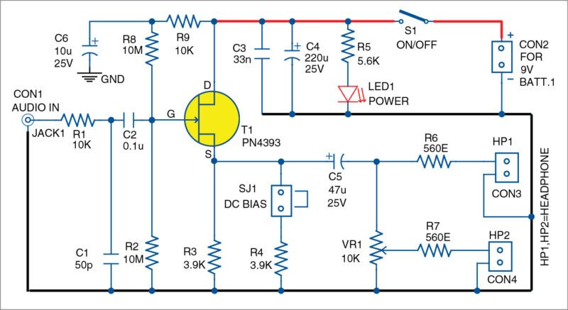
Fig. 1: Circuit diagram of the high-impedance audio buffer with JFET
Audio input is applied to connector CON1. Input impedance depends mainly on the values of resistors R2 and R8 and is around 5-mega-ohm. If resistors R8 and R9 and capacitor C6 are omitted, input resistance will depend mainly on R2 and will be around 10-mega-ohm.
Value of R2 can be increased but it may be difficult to maintain the high input resistance during the practical usage of the circuit. Resistor R1 and capacitor C1 are used for protection and filtering functions for the input of the buffer, respectively. C1 can be omitted but not R1. Values of R1 and C1 can be changed as per requirement. Capacitor C2 is used to remove DC input components.
Resistors R8 and R9 between gate G and drain D of transistor T1 are not always needed. So resistor R8 is not necessarily equal to R2. Also, R8 will reduce the input impedance. Use of high-value resistors R2 and R8 may increase input noise, so care must be taken while selecting their values.
Resistor R9 and capacitor C6 are for filtering noise from the power source. These can be omitted if the power source is clean. But filtering capacitors C3 and C4 should not be omitted.
Resistors R3 and R4 provide DC bias for the JFET. Resistor R4 is connected to transistor T1 through shorting jumper SJ1. Range of R3 is from 1-kilo-ohm to 10-kilo-ohm. Lower values will provide lower output impedance but will increase the power consumption. Bias depends on the input signal, parameters of the JFET and power supply.
JFETs have wide tolerances, which is the main issue during their application. Fortunately, this is not a problem here. If a single circuit is required, choose an appropriate value for R3 depending on the JFET. In that case, SJ1 and R4 can be omitted. If some other JFET devices are required, connect R4 to source S of the JFET through SJ1 without changing the value of R3 to adjust the circuit to the parameters of the JFET.
This buffer has two outputs available at connectors CON3 and CON4. The outputs can drive loads of 10-kilo-ohm or more, simultaneously. Higher impedance loads are preferred. The loads can be reduced to 2-kilo-ohm without overloading the circuit, but amplitude of the signal will drop. Usually, that is not a problem. The circuit can drive two high-impedance 2-kilo-ohm headphones (HP1 and HP2) connected to CON3 or CON4 (a total load of 4-kilo-ohm).
Signal level on output CON3 is not adjustable but signal level on CON4 is, using potmeter VR1.
Choice of power supply depends on the peak-to-peak amplitude from the signal source. One or two 9V batteries of type 6F22 can be used. These provide 9V or 18V of power supply voltage, covering practically all passive pickups for the musical instruments and other high-impedance sensors. Some JFETs allow higher power supply. A well-filtered DC wall adaptor can also be used.
Construction and testing
An actual-size, single-side PCB for the high-impedance audio buffer with JFET is shown in Fig. 2 and its component layout in Fig. 3.
Fig. 2: Actual-size PCB layout for the high-impedance audio buffer with JFETFig. 3: Component layout of the PCB
This circuit may require appropriate selection of values of resistors R3 and R4 in order to optimise the peak-to-peak amplitude of the output signal. It is appropriate for battery operation, which is important for portable applications.
The circuit can be mounted in a small box near the pickup or attached to the strap of the string instrument. Due to its high input impedance, input cable should be shorter than one metre and shielded or, at least, twisted. The gain is lower than unity but that is not a problem because most pickups provide strong signals.
Petre Tzv Petrov was a researcher and assistant professor in Technical University of Sofia (Bulgaria) and expert-lecturer in OFPPT (Casablanca), Kingdom of Morocco. Now he is working as an electronics engineer in the private sector in Bulgaria
Automation systems are increasing in day to day life. Applications like home and industrial automation reduce man power while increasing the efficiency. Here in this project let us see how automated menu for ordering food in restaurants can happen.
In these modern days the number of restaurants are increasing. They also require very fast processing for serving food to the customers. With the increasing number of customers, it would require more man power, since the current situation has become hectic for the restaurants. Also changes in the hardcopy of the menu can’t happen.
Using simple components and programming techniques, an automation system was proposed.
Circuit Explanation
Restaurant automation system consists of a transmitter and a receiver section.
Atemga8 is the AVR microcontroller used for processing the data. The above circuit does not show any clock or reset circuit. For normal operation of the controller reset should be connected to high logic.
Vcc and ground should also be connected to the circuit, which are not shown in the above circuit. It has two ground pins (pin 8 &pin 22). Vcc is connected to 5V and a Vcc is used for A/D conversion. Below is the image showing reset and power connections to the controller.
No need of external crystal, it can work with internal oscillator of 8MHz.
Transmitter:
• Transmitter section is used for ordering from the menu.
• A 4X3 keypad is used to select the items. Four rows of the keypad are connected to PORT C of the microcontroller, while the three columns are connected to PORT D.
• Zigbee transmitter is connected to the transmit and receive pins of the microcontroller. Here the transmitter pin of the microcontroller is connected to the transmitter of the zigbee transmitter module. No need of connecting receive pin, as the module only transmits the data.
• LCD is also connected in order to view the selected items. Here LCD is used in 4 bit mode.
Receiver:
• The receiver section is connected in the kitchen. The order placed by the customer is received by the zigbee receiver. In real one can form a zigbee network in which single receiver is used to receive data from different transmitters.
• Thus received data is decoded and is displayed on the LCD .
Working
• The menu is displayed on the LCD .
• User should press the corresponding number of the selected item from the display.
• The project code is provided below. It is written in such a way that one can select 3 items at a time. In real time one can use EEPROM of the microcontroller to store the menu.
• Items are selected using keypad provided. For example in order to select “1. Ice cream” press 1 one from the keypad. Similarly select your items and press ‘#’ .
• Pressing ‘#’ will transmit the order to the receiver.
Arduino is very helpful for people who have little knowledge of programming or electronics. The user does not need to understand the hardware or the low level coding of the AVR controller.
Arduino is easy to use and can be learned with very little effort. Hence, the development/prototyping time using Arduino is considerably less. Arduino is based on WinAVR, a gcc compiler for AVR. You can create an Arduino project in Atmel Studio and even simulate it.
At present Arduino uses ATmega328, ATmega168, ATmega1280, ATmega2560 and ATmega8 boards/controllers. However, many users/developers are using ATmega32 controller in their projects now and are more familiar with this controller. But it is not seen in the list of Arduino boards in Arduino IDE.
ATmega32 has 32 general-purpose input/output (GPIO) pins, which is more than 20 used in ATmega328. It is disappointing that some boards have more I/O pins, like ATmega1280 and ATmega 2560, but are expensive.
In this project, we use ATmega32 as a microcontroller (MCU) in Arduino board and utilise almost all the 32 GPIO pins available as shown in Fig. 1. Author’s prototype is shown in Fig. 2.
Fig. 1: Pin details of ATmega32Fig. 2: Author’s prototype on the board
Pinout of ATmega32 as used in Arduino board
1. Thirty two digital pins (D0 to D31)
2. Eight analogue-to-digital pins (A0 to A7); these can be used as digital pins also
3. Four PWM pins
4. Other pin details in Fig. 1
Circuit and working LCD interface. Normally, Arduino boards do not have an LCD on board. However, for development work it is very essential. Provision of an onboard LCD is very easy because no extra wiring or component is required; only data pins are to be connected.
Push-to-on switches.Four push-to-on switches are provided onboard for testing purpose; no extra wiring is required, hence testing is fast and easy.
LEDs.Four LEDs are provided onboard for easy and fast testing.
Buzzer.This is provided to test sketches using tones in Arduino.
Power supply. Vcc and ground pin headers (four pins each) are provided for extending the supply voltage and ground pins while testing.
Other provisions.All other provisions like digital pins and analogue pins are available as on any other Arduino board.
The detailed circuit diagram of Arduino for ATmega32 is shown in Fig. 3.
Fig. 3: Circuit diagram of Arduino for ATmega32
Software
Arduino software version 1.0.5 has some directories. For making it suitable for ATmega32 we have to modify/add some directories/files to it. The directory structure is given in Fig. 4.
Fig. 4: Directory tree of Arduino 1.0.5 IDE
Check which directory/file needs to be modified/added. Details of modifications, that is, where/which lines are to be changed/added are given here for reference.
But first make a copy of Arduino version 1.0.5 software and make required changes in it. If you do not have 1.0.5 version, go to www.arduino.cc and click Download Link. From Previous Release box click Arduino 1.0.x and then click Windows option for version 1.0.5. Save this file and expand it.
Follow the instructions given below for making modifications: Directory structure of Arduino.Go through it and verify it with Arduino version 1.0.5 so that you get overall idea of the changes required in the files and folders of Arduino. For editing relevant files (like boards.txt, pins_arduino.h and so on), use Programmer’s Notepad and use/toggle line number display so that you can view line numbers in the opened file.
Modify the files in this directory structure as per the steps below.
Go to Hardware\Arduino directory.Open the text file named boards.txt and add the following lines at the end of this file:
Define the hardware of ATmega32.For this, search for directory location hardware\arduino\varients and create a new directory named mega32. Inside this new directory, add a new file named pins_arduino.h by copying it from Standard Directory.
This file includes digital pins, analogue pins, timer pins, pwm pins, ports and port bits. The numbers of digital pins, analogue pins and pwm pins are changed as below:
Pin change interrupt (PCINT) is removed as it is not applicable for ATmega32. Constants are changed, that is, change for SS, MOSI, MISO, SCK, SDA and SCL as per ATmega32 hardware pin out.
Search for hardware\arduino\cores\arduino directory. Open Arduino.h file and add the following line after the last timer-defined line, that is, after #define TIMER5C 17, which comes after line number 184.
#define TIMER0 18
Open Tone.cpp file in the cores directory and add/modify the following to suit Timer2 of ATmega32.
After line number 39, add defined(__AVR_ATmega32__) as shown below:
These modifications are sufficient. You can now select Arduino ATmega32 under Tools>Board on Arduino IDE 1.0.5 as shown in Fig. 5. You may perform all the steps for ATmega32 on this IDE like any other Arduino board. But with this you cannot load the sketches without an external programmer because we have not loaded bootloader on ATmega32 yet.
Fig. 5: Arduino ATmega32 board under Tools menuFig. 6: Hex file for Arduino ATMEGA32 under build in C://
However, without the bootloader, it is also advantageous as full memory space is available for sketches\application programs on ATmega32. If we use bootloader, it will consume 2k memory of ATmega32.
With this project, you can use Arduino IDE for various designing purposes using ATmega32 MCUs.
Construction and testing
An actual-size, single-side PCB pattern of Arduino on ATmega32 circuit is shown in Fig. 7 and its component layout in Fig. 8. Assemble the circuit on the PCB as it minimises time and assembly errors. Carefully assemble the components and double-check for any error(s). Use proper IC base for the MCU. Test different programs like digital read, analogue read, LCD display, serial display, tone, etc using ATmega32 for Arduino with all 32 GPIO pins.
Fig. 7: Actual-size PCB layout of Arduino for ATmega32Fig. 8: Component layout of the PCB
The hex file generated (after compiling the sketch for Arduino board using ATmega32) on Arduino 1.0.5 IDE can be obtained by searching the build folder in C:// as shown in Fig. 6.
You may connect an external programmer to CON3 in Arduino ATmega32 board to burn the hex file into ATmega32.
You can also change any future version of Arduino for ATmega32 once you understand how to change the corresponding files in that version.
Federal and international regulations require boats to carry lights between sunset and sunrise and during conditions of restricted visibility. The number and colours of the lights vary with the size of the vessel.
Many commercial vessels carry special lights that identify them to the others. This is important because right of way depends on the types of vessels involved. Tugs and commercial fishing vessels have the right of way over sailboats, which have the right of way over ordinary power vessels.
Fig. 1: Anchor light position at the top of a mast
Unique lights are carried by each one. For example, when you are anchored (or tied to a mooring ball), you must display an anchor light that is a white all-around light. It needs to be mounted high so it can be seen from a distance (refer Fig. 1).
However, most of the cruisers do not use a masthead anchor light because the light is too high above the water level and actually makes it difficult to judge the position of the boat from just the anchor light, especially in a pitch-dark anchorage. That is why many people have devised their own forms of anchor lights that they stick lower to the deck on both sides of their boat.
Fig. 2: A typical commercial anchor light
Here is the circuit of a compact yet inexpensive automatic anchor light integrated with an ambient light sensor that turns it on and off automatically. This 12-volt LED anchor light can be used as a traditional masthead anchor light and/or as an optional pretty clever custom-built anchor light. A typical commercial anchor light is shown in Fig. 2.
Circuit and working
The circuit described here (refer Fig. 3) lets you control an electromagnetic relay so that it turns on a white LED light when the preset light level is reached and turns it off when a different preset level is reached. The circuit is built around NE555 IC (IC1). The 5mm light dependent resistor (LDR1) in the circuit triggers the 12V electromagnetic relay (RL1) as per the ambient light level. RL1 drives the 10mm white LED light source (LED2). Series resistor (R2) is included to limit the white LED current.
Fig. 3: Circuit diagram of the anchor light
Note that switching threshold is determined by a 470k potentiometer (VR1) that causes the output to toggle with the preset threshold values. The light source (LED2) automatically switches on when it gets dark and switches off when there is sufficient ambient light. The 100µF capacitor (C1) provides a bit of hysteresis to prevent the circuit from jittering near the threshold level. The circuit is optimised for use with a nominal DC voltage of 12V drawn from any standard accumulator commonly used in boats.
Construction and testing
An actual-size, single-side PCB pattern for the anchor light circuit is shown in Fig. 4 and its component layout in Fig. 5.
Fig. 4: Actual-size PCB pattern of the anchor light circuitFig. 5: Component layout of the PCBFig. 6: Suggested enclosure layout
The circuit assembled on the small PCB can fit easily inside most prototype/custom enclosures, which should be waterproof for mounting on the masthead. If possible, try to add some optics (lens and reflector) with the white LED (LED2) to spread the light outward. The 12V power supply input wires can then be connected to corresponding wires extending from the existing electric-points of the anchor light. Fig. 6 shows how the prototype may be assembled. Author’s prototype is shown in Fig. 7.
Fig. 7: Author’s prototype
T.K. Hareendran is founder and promoter of TechNode Protolabz
Raspberry is a development board that has made a lot of noise since its introduction to the public. The cost and the wide support community has further added to the wide range of applications this board supports. Let’s take a look at the top 20 Raspberry Pi project ideas for you to get busy with.
Before we go into designing projects, let’s configure that little board first. This project takes you through understanding the project and lists out on some of the basic requirements which being:
a secure home network.
a router that can accept a direct ethernet cable.
If you are working at an office, the network configuration settings outlined here might have to be adapted for your specific company’s network/firewall.
Security has been a major concern with a lot of people living in the big cities. Even if you are not in a major cities, security is still a concern. A lot of people want their hands on what is not theirs. The surveillance camera is based on a raspberry pi board and uses Wi-Fi for transmission of captured signals.
Once you know nobody can enter your home without being caught on camera. You can go ahead with feeling a bit safer. This next project let’s you make your very own media centre right in your house, to enjoy some of your new found safety. The project takes you through the various steps involved with designing the system using a raspberry pi. Probably you could have a dance-off over the weekend as well.
With the surveillance camera project you could know who is coming in, but how do you track your family? After all, there is a danger of them dropping by unannounced. With this next project you could build a system that uses GPS over a raspberry pi to help you track targets. Now don’t go all Bond and start tracking every person you know. Everybody has a right to their privacy as well.
Once all the fun and games are over, you might want to get down to business. Raspberry pi let’s you setup a web server from the comfort of your own home. This next project, takes you through setting up a web server for WordPress on Raspberry Pi. WordPress is a PHP and MySQL based open source blogging platform and content management system. With the huge support community, this should be a blast to work on.
This project is an FM receiver circuit radio based on Philips TEA5767 digital radio-receiver module. The radio receiver uses I2C interface with Arduino UNO development board. The TEA5767 module offers such features as stereo or mono outputs, radio station scanning and signal strength indication. The author’s prototype on a breadboard is shown in Fig. 1.
Fig. 1: Author’s prototype
Circuit and working
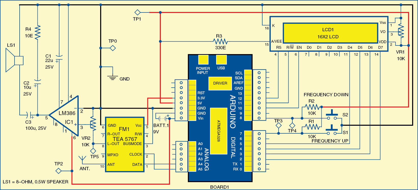
The circuit of the Arduino-based FM receiver, shown in Fig. 2, is built around Arduino UNO board (board1), TEA5767 radio receiver module (FM1), LM386 low-power amplifier (IC1), 16×2 LCD (LCD1) and 8-ohm speaker (LS1).
Arduino UNO board
Arduino is an open source electronics prototyping platform based on flexible, easy-to-use hardware and software. It is intended for artists, designers, hobbyists and anyone interested in creating interactive objects or environments.
Fig. 2: Circuit diagram of the Arduino-based FM receiverFig. 3: TEA5767 digital radio receiver module
Arduino UNO is a board based on ATmega328 microcontroller. It has 14 digital input/output pins, six analogue inputs, a USB connection for programming the on-board microcontroller, power jack, an ICSP header and a reset button. Operation is with a 16MHz crystal oscillator and contains everything needed to support the microcontroller. It is easy to use as the user simply needs to connect it to a computer with a USB cable, or power it with an AC-to-DC adaptor or battery, to get started. The microcontroller on the board is programmed using Arduino programming language and Arduino development environment.
Pins A4 and A5 of the Arduino board are connected to DATA and CLOCK pins of the FM module (FM1), respectively. 10 through 12 pins of the Arduino board are connected to EN, R/W and RS pins of LCD1 while pins 2 through 5 are connected to data pins of the LCD. Pins 7 and 8 of the Arduino board are connected to tactile switches S1 and S2 to increase and decrease FM frequency, respectively.
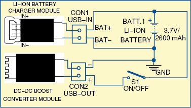
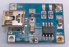
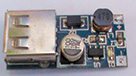
This power bank can be used for charging smartphones. The circuit uses two integrated modules and a lithium-ion battery. The first module is a lithium-ion battery charger and the second is a DC-DC boost converter module.
Circuit and working for power bank
Circuit diagram of the power bank is shown in Fig. 1. It consists of a USB lithium-ion charger module (USB-IN), 3.7V/2600mAh lithium-ion battery (BATT.1), on/off switch (S1) and DC-DC boost converter module (USB-OUT).
Fig. 1: Circuit diagram of the power bank
Here, a lithium-ion charger module based on TP4056 IC, rechargeable lithium-ion battery (Samsung type 18650) and DC-DC converter module based on pulse frequency modulation (PFM) technology are used.
The battery charger module, shown in Fig. 2, is designed around a dedicated lithium-ion battery charger TP4056 chip and populated with SMD components. This onboard charge controller chip handles BATT.1 charging operation by processing the 5V DC input supply received through the USB socket (or through IN+ and IN- terminals). Output terminals (BAT+ and BAT-) can be directly connected to BATT.1. Two onboard SMD LEDs located on top of the circuit board provide charging-status indications.
BATT.1 is used as the power reservoir. Since only 3.7V DC supply is available from BATT.1, DC-DC boost converter is used to cater to the stable 5V DC supply at output. If input voltage of 0.9V to 5V DC is available, this converter gives stable 5V DC output through its USB socket, with conversion efficiency up to 96 per cent.
The DC-DC boost converter module, shown in Fig. 3, is an SMD module with a PFM chip at its heart. Input DC supply fed through input terminals (+ and -) is processed by this dedicated chip to give a stable USB standard DC supply via the standard USB socket at its output. An onboard SMD LED, fitted near the input terminals, works as a power-status indicator. Switch S1 is included to route DC supply from BATT.1 to the converter.
Operation application
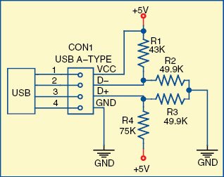
Almost all smartphones look for signals/levels on D+ and D- of the USB interface that indicate the charger’s current capability. A full-speed device will use a pull-up resistor attached to D+, as shown in Fig. 4, to satisfy itself as a full-speed device. The pull-up resistor at the device end will also be used by the host or hub to detect the presence of a device connected to its port. Without this resistor logic, the USB assumes there is nothing connected to the bus.
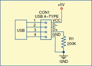
In case of a charging error, pull down D+ line of the USB output socket (in converter module) with the help of a 200-kilo-ohm resistor as shown in Fig. 5.
Fig. 4: Pull-up resistor configuration at D+ and D- pinsFig. 5: Pull-down resistor configuration at D+ pin
Construction and testing
Assemble all components of the power bank circuit as per Fig. 1. Follow the testing operation given below:
1. Connect the charger module to CON1 (USB-IN) either through an AC adaptor or provide 5V DC supply through a PC or laptop using a USB cable for charging BATT.1.
2. Connect BATT.1 across CON1 for charging. A red-coloured LED will turn on, showing the charging status of BATT.1. When the battery is fully charged, a blue-coloured LED will turn on. You may remove the charger connected at USB-IN.
3. You can now charge your smartphone by connecting it to the USB socket of the converter module (USB-OUT) using a USB cable and closing switch S1. A red-coloured LED of the converter module will turn on, showing the charging status of the smartphone.
EFY note. Connect the terminals of BATT.1 to USB-IN and USB-OUT with correct polarity.
T.K. Hareendran is an electronics hobbyist, freelance technical writer and circuit designer
A radio receiver is an electronic device that receives radio waves and converts the information carried by them to a usable form. An antenna is used to catch the desired frequency waves. The receiver uses electronic filters to separate the desired radio frequency signal from all the other signals picked up by the antenna, an electronic amplifier to increase the power of the signal for further processing, and finally recovers the desired information through demodulation.
Of the radio waves, FM is the most popular one. Frequency modulation is widely used for FM radio broadcasting. It is also used in telemetry, radar, seismic prospecting, and monitoring newborns for seizures via EEG, two-way radio systems, music synthesis, magnetic tape-recording systems and some video-transmission systems. An advantage of frequency modulation is that it has a larger signal-to-noise ratio and therefore rejects radio frequency interference better than an equal power amplitude modulation (AM) signal.
FM frequency ranges
Frequency modulation is used in radio broadcast in the 88-108MHz VHF band. This bandwidth range is marked as FM on the band scales of radio receivers, and the devices that are able to receive such signals are called FM receivers. The FM radio transmitter has a 200kHz wide channel. The maximum audio frequency transmitted in FM is 15 kHz as compared to 4.5 kHz in AM. This allows much larger range of frequencies to be transferred in FM and thus the quality of FM transmission is significantly higher than of AM transmission. Presented below is electronics circuit for FM receiver along with its full explanation.
List of Components
IC- LM386
T1 BF494
T2 BF495
4 turn 22SWG 4mm dia air core
C1 220nF
C2 2.2nF
C 100nF * 2
C4 10uF
C5 10uF (25 V)
C7 47nF
C8 220 uF(25 V)
C9 100 uF (25 V) * 2
R 10KΩ * 2
R3 1KΩ
R4 10Ω
Variable resistance
Variable capacitance
Speaker
Switch
Antenna
Battery
FM receiver circuit explanation
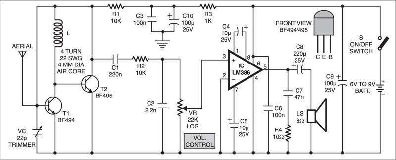
Here’s a simple FM receiver with minimum components for local FM reception. Transistor BF495 (T2), together with a 10k resistor (R1), coil L, 22pF variable capacitor (VC), and internal capacitances of transistor BF494 (T1), comprises the Colpitts oscillator. The resonance frequency of this oscillator is set by trimmer VC to the frequency of the transmitting station that we wish to listen. That is, it has to be tuned between 88 and 108 MHz. The information signal used in the transmitter to perform the modulation is extracted on resistor R1 and fed to the audio amplifier over a 220nF coupling capacitor (C1).
Fig.1: FM Receiver Circuit Diagram
You should be able to change the capacitance of the variable capacitor from a couple of picofarads to about 20 pF. So, a 22pF trimmer is a good choice to be used as VC in the circuit. It is readily available in the market. If you are using some other capacitor that has a larger capacitance and are unable to receive the full FM bandwidth (88-108 MHz), try changing the value of VC. Its capacitance is to be determined experimentally.
The self-supporting coil L has four turns of 22 SWG enamelled copper wire, with air core having 4mm internal diameter. It can be constructed on any cylindrical object, such as pencil or pen, having a diameter of 4 mm. When the required number of turns of the coil has reached, the coil is taken off the cylinder and stretched a little so that the turns don’t touch each other.
Capacitors C3 (100nF) and C10 (100µF, 25V), together with R3 (1k), comprise a band-pass filter for very low frequencies, which is used to separate the low-frequency signal from the high-frequency signal in the receiver.
Antenna is a bit tricky
You can use the telescopic antenna of any unused device. A good reception can also be obtained with a piece of isolated copper wire about 60 cm long. The optimum length of copper wire can be found experimentally.
The performance of this tiny receiver depends on several factors such as quality and turns of coil L, aerial type, and distance from FM transmitter. IC LM386 is an audio power amplifier designed for use in low-voltage consumer applications. It provides 1 to 2 watts, which is enough to drive any small-size speaker. The 22k volume control (VR) is a logarithmic potentiometer that is connected to pin 3 and the amplified output is obtained at pin 5 of IC LM386. The receiver can be operated off a 6V-9V battery.
Most remote controls around us, use IR for signal transmission. An IR remote control for home appliances helps you connect to your decices at ease and operate them from the comfort of your bed or your chair. Here we try to build an IR remote control for home appliances that you can use in your home. Using this circuit, you can remotely control the switch-on and switch-off operation of your AC mains operated home appliances. The working range of the circuit depends on the orientation and the intensity of the IR beam.
IR remote control for home appliances: Transmitter circuit
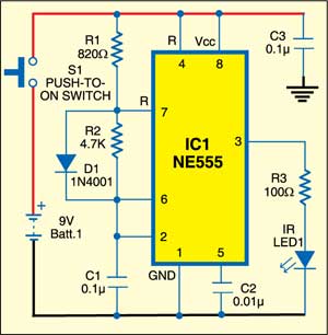
Fig. 1: Transmitter circuit
Fig. 1 shows the transmitter circuit. It is built around timer IC NE555 wired as an astable multivibrator. The multivibrator produces a pulsed output waveform with ‘on’ time of about 57 µs and ‘off’ time of about 326 µs, which means it generates about 2.6 kHz. The output of IC1 is fed to IR LED1 through current-limiting resistor R3. The IR LED1 used here is the same as in TV remotes. The circuit operates off a 9V battery, which is connected to the circuit through switch S1.
IR remote control for home appliances: Receiver circuit
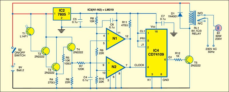
Fig. 2 shows the receiver circuit. It consists of phototransistor L14F1 (T1), voltage regulator 7805 (IC2), three 2N2222 transistors (T2, T3 and T4), dual voltage converter LM319 (IC3), dual J-K flip-flop 74109 (IC4) and some discrete components. The circuit operates off a 9V battery, which can be connected to the circuit through switch S2.
The Darlington pair built around transistors T2 and T3 amplifies the photo-current generated by the photo-transistor (T1). The equivalent photo-voltage appears across resistor R4. So across resistor R4 you get a replica (in term of wave shape but not in amplipude) of what you produce at the output of IC1 in the transmitter. The amplitude would vary with distance and other factors such as the angle of arrival of the IR beam at sensor L14F1.
Fig. 2: Receiver circuit
The low-pass filter constituted by resistor R7 and capacitor C4 produces about 3V DC. This DC voltage is fed to the junction of the inverting input of N1 and the non-inverting input of N2. The window comparator (IC3) is designed such that whenever the input voltage is between 2 and 4 volts (greater than 2V but less than 4V), its output goes high. If the input voltage is less than or equal to 2V, or more than or equal to 4V, the output goes low.
The window output is fed to the clock input of J-K flip-flop CD74109 (IC4). IC4 is wired in toggle mode. That means its output goes high if it is initially low and vice versa every time it is clocked. The output of IC4 is fed to the base of relay-driver transistor T5. Relay RL1 energises to light up the bulb when transistor T5 conducts.
Circuit working
Working of the circuit is simple. Initially, when no IR beam is falling on sensor photo-transistor T1, the DC voltage appearing at the input of the window comparator is nearly zero. The window output remains low. Transistor T5 is cut-off and the relay remains de-energised.
When switch S1 is pressed momentarily, the IR beam falls on the photo-transistor for this short period of time and a postive-going pulse appears at the input of the window comparator. The output of the comparator goes low, which toggles the flip-flop (IC4) and transitor T5 conducts. Relay RL1 energises to switch on bulb B1.
Assemble both the circuits on separate PCBs and house in suitable cabinets. In the transmitter unit, fix IR LED1 on the front side and switch S1 on the back side of the cabinet. Keep the 9V battery inside the cabinet.
Similarly, in the receiver unit, fix the photo-transistor (L14F) on the rear side such that the IR beam falls on it. To avoid circuit malfunction, cover the phototransistor (T1) with a suitable contraption so that the phototransistor is not exposed to unwanted light sources. Fix switch S2 on the front panel and the relay on the back side. Keep the 9V battery inside the cabinet.
Most of the circuits for intelligent level controller for water in tanks employ a bunch of wires running between the circuit and the overhead tank, which accounts for almost half the cost of the entire project. Here is an intelligent scanned water-level indicator-cum-pump controller circuit (Fig. 1) that utilises just four wires to the overhead tank to indicate nine different levels.
Circuit diagram for the intelligent level controller
The connection arrangement for the overhead tank (OHT) and the underground tank (UGT) is shown in Fig. 2. Two wires from the circuit in Fig. 1 run to the underground/ground-level tank (to output line K and return line J, respectively) to check the availability of water in the tank before operating the pump, thereby guarding the pump against the damage due to dry running.
The scanning section employs an NE555 timer (IC1) wired as an astable multivibrator to oscillate at around 1 kHz. The output of NE555 is connected to CLK inputs of two CD4017 Johnson counters (IC2 and IC8). (IC8 is placed near the overhead tank in Fig. 2.)
Working
Suppose at a given time, there is some specific water level in the OHT. The clock from NE555 keeps advancing the Q outputs of IC2 and IC8 starting from Q0. Only when the Q output of IC8 corresponding to the first (starting from top) water-submerged probe goes high, the OHT RET line goes high through water in the OHT. This causes pins 2, 5, 10, and 13 of quad AND gate ICs (IC3 and IC4) as well as one input of AND gate A2 to go high via emitter-follower transistor T2. The identical Q output of IC2 goes high simultaneously to light up the corresponding LED (LED1 through LED9) to indicate that particular level.
Similarly, upon reception of the next clock, the next lower level is indicated by the next LED, and so on. Scanning at a very high speed gives the illusion that all LEDs up to the one corresponding to the actual level in the OHT are continuously lit. This is due to the persistence of vision.
Connections
Fig. 2: Connection arrangement for overhead and underground tanks
When the water level in the OHT is high enough to light up LED1, both the inputs of AND gate A1 also go high simultaneously. As a result, the output of AND gate A1 goes high to reset the flip-flop IC (IC5). The output pin 2 of IC5 goes low to de-energise relay RL1. Now when the water level in the OHT goes low such that LEDs 1 through 9 are off, the output of AND gate A3 goes high to set RS flip-flop (IC5), thereby making its output pin 2 high. Only when there is enough water in the UGT, pin 12 of AND gate A4 will be at logic 1 to provide forward bias to relay driver transistor SL100 (T3) to energise the relay to switch on the pump motor.
The motor will switch off only when the water level reaches the uppermost level or when the UGT gets empty. LED10 through LED12 indicate ‘motor off’, ‘motor on’, and ‘UGT empty’, respectively. IC8 is powered separately, using a 9V battery that lasts long enough.
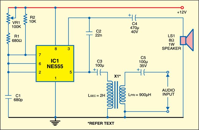
The “555” integrated circuit is a general-purpose timer useful for a variety of functions. In this 555 audio PWM project, we explore its use as an astable multivibrator. The ubiquitous 555 timer IC handles audio signals in its own pulse-width modulation (PWM) way. Here, the 555 IC works in astable mode. The switching frequency can be varied from 65 kHz to 188 kHz. Selection of PWM frequency depends on the amplitude of the input signal as well as the load impedance. By adjusting VR1, you can ensure comfortable listening with low audio distortion.
Working explanation
In pulse-width modulation, the carrier frequency’s pulse width varies as a function of the amplitude of the input audio signal. Feedback capacitor C2 ensures faithful reproduction of the audio signal. An output L-C filter is the common approach for a reasonable rejection of the carrier frequencies. For simplicity, it is omitted here. Moreover, the speakers cannot respond to the high-frequency signal. They respond to the average DC level modulated with the audio signal that we feed in from the input. Of course, the audio quality is not as good as that of a professional system, but it would be definitely an amazing experience to listen audio through a 555 chip with room-filling volume.
555 Audio PWM circuit
Impedance matching at both the input and output is important. So an input-impedance matching transformer (X1) is used to match the headphone output of a standard CD player to the input of the 555 amp. 8-ohm, 1W speakers were used as the load. If designed properly, PWM amplifiers could give a performance similar to conventional amplifiers. Even higher efficiency and effortless bass are possible.
EFY note.While testing this circuit at EFY lab, we had used Supertronix KEC make matching transformer X1, and the input to the circuit was the audio output taken from the computer’s headphone out terminal.
 RS232 signals cover a much longer distance than standard TTL and I2C signals. Also, RS232 signals have better noise immunity. RS232 is a well-known standard supported by many popular integrated circuits (ICs) and therefore is still widely used. Sometimes we want to send TTL and I2C signals over a longer distance. This article describes how these signals can be extended through RS232 lines.


 With daylight falling on LDR1 (dawn mode), resistance of LDR1 becomes low, a small current flows through LED1 and it glows. At the same time, due to low voltage across LDR1, MOSFET IRF640 does not trigger. So load (LED light/inverter) remains off.
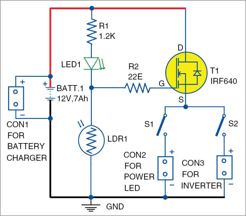
 The circuit for an LPG leakage detector is readily available in the market, but it is extremely expensive and usually based on a microcontroller (MCU). Presented here is a low-cost circuit for an LPG detector that you can build easily.
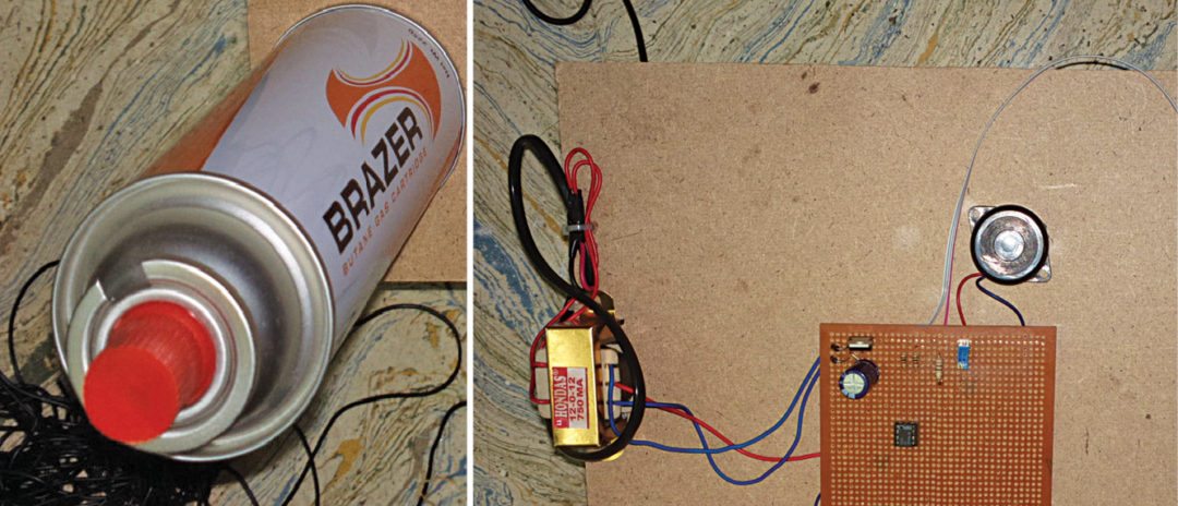
 The mains supply is stepped down by transformer X1, rectified by a full-wave rectifier comprising diodes D1 and D2, filtered by capacitor C1 and fed to regulator 7805 (IC1) to maintain constant 5V DC output, which is fed to the circuit.
 A thermostat is a standard equipment for sensing temperature of a system and maintaining it at a pre-defined point. It is a regular feature in air-conditioners, room heaters and refrigerators. Although some commercially-available refrigerators have inbuilt thermostats, the given circuit is easy to build and automatically turns on or turns off the appliance at pre-set temperatures.
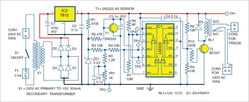


 Additive mixing of red and green lights produces shades of yellow, orange or brown. Mixing green and blue produces shades of cyan, whereas mixing red and blue produces shades of purple including magenta. Mixing nominally equal proportions of the three primaries results in shades of grey or white; colour space that is generated is called an RGB colour space.
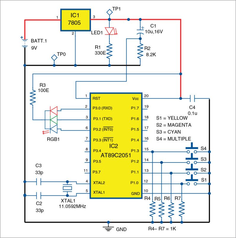
 When the circuit is switched on, red colour of the RGB LED glows for a preprogrammed time interval of three seconds. It then switches off for three seconds. This is followed by green and blue colours switching on and off in a similar manner and for the same time periods.
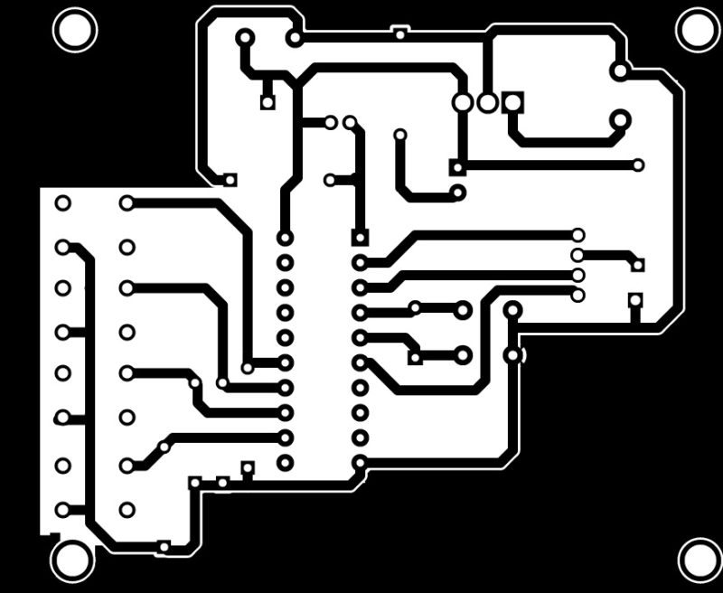
 Op-amps require dual-polarity supply for proper operation. When working with battery supply, it becomes difficult to get dual power supply for the op-amps. Presented here is a simple circuit that provides ±5V from a 9V battery.
 The circuit diagram for the ±5V supply from a 9V battery is shown in Fig. 1. It is built around 9V battery (BATT.1), voltage regulator IC 78L05 (IC1), CMOS voltage converter ICL7660 (IC2) and a few other components.
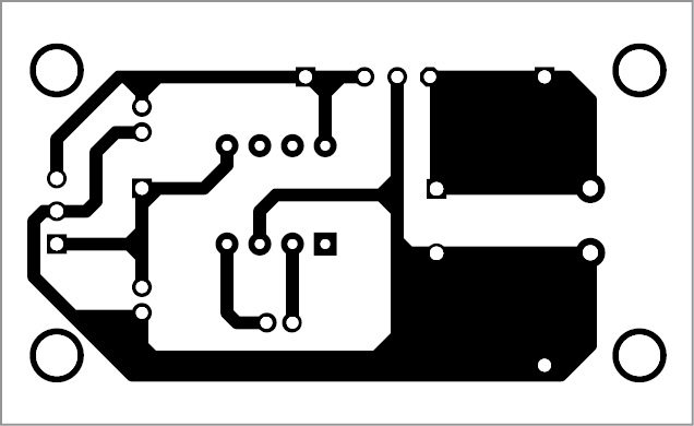
 It detects visible light and infrared (IR) in the range of 430nm – 1100nm. So visible light and IR from the fire can easily activate the sensor to trigger the alarm. It also detects sparks in the mains wiring and, if these persist, it gives a warning alarm.
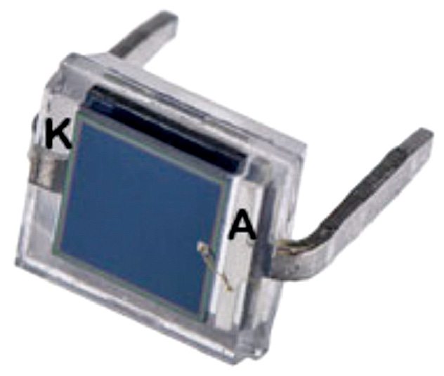
 Resistors R8 and R9 between gate G and drain D of transistor T1 are not always needed. So resistor R8 is not necessarily equal to R2. Also, R8 will reduce the input impedance. Use of high-value resistors R2 and R8 may increase input noise, so care must be taken while selecting their values.


 Arduino is very helpful for people who have little knowledge of programming or electronics. The user does not need to understand the hardware or the low level coding of the AVR controller.


 What is a FM receiver?