Quantcast
Viewing all 48 articles
Browse latest View live

Audio Mixer with Multiple Controls

Image may be NSFW.
Clik here to view.
When recording sound from several orchestral instruments being played by different musicians using a single microphone, the only way to adjust the sound balance is to change the position of the musicians relative to the microphone. When recording direct to stereo master tape, it’s crucial to make sure that all the voices and instruments sound right before you hit the record button. Presented here is an eight-input audio mixer circuit with bass, treble, volume and balance controls, which you can use to balance sounds from all the sources until you have the desired mix. For capturing the sound from various sources, the audio mixer employs up to eight microphones.
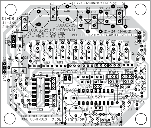
Audio mixer circuit

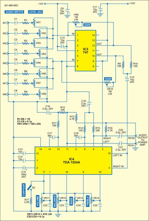
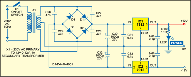
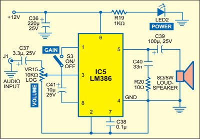
Fig. 1 shows the block diagram of the audio mixing system along with the audio power amplifier, while the circuit of the audio mixer along with tone controller is shown in Fig. 2. The power supply and audio power amplifier circuits are shown in Figs 3 and 4, respectively.

Image may be NSFW.
Clik here to view.
Fig. 1: Block diagram of the audio mixer with bass, treble, volume and balance controls

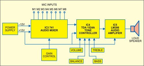
Here, dual operational amplifier IC 747 (IC3) is used for mixing several inputs without any mutual interaction. The two internal amplifiers share a common bias network and power supply. The IC has short-circuit protection and wide common-mode and differential voltage ranges.

In this application, +12V and –12V regulated DC supplies are used for operation of IC 747. The microphone output signals M1 through M4, after their individual level adjustments, are mixed and applied across the differential input terminals (pins 1 and 2). Similarly, microphone outputs M5 through M8 are applied across the differential input terminals (pins 7 and 6) of the second amplifier inside op-amp IC 747 after their individual level adjustments.

Image may be NSFW.
Clik here to view.
47C_part-list

Circuit operation

For level adjustment, logarithmic variable resistors VR1 through VR4 and VR5 through VR8, respectively, are employed while feeding the output from respective microphones to the input of the two amplifiers inside IC 747. The outputs of the two amplifiers taken from pins 12 and 10, respectively, are combined at the junction of resistors R9 and R10 before feeding to the next stage (tone controller) via capacitor C12 (10 µF). The overall gain of individual amplifiers can be adjusted with the help of potmeters VR9 and VR10, respectively.

The amplified mixed signal output of IC 747 is applied to shorted input pins 15 and 4 of stereo tone controller IC TDA1524A (IC4). TDA1524A is designed as an active stereo-tone/volume control for car radios, TV receivers and mains-fed equipment. It includes functions for bass and treble control, volume control with built-in contour (can be switched off) and balance. All these functions can be controlled by DC voltages or by single linear potentiometers. This IC serves as an efficient tone controller. Although it may work reasonably well with 9V DC supply, for better bass response, a 12V supply can be used. A good heat-sink is necessary for longer life and better performance of the IC.

Image may be NSFW.
Clik here to view.
Fig. 2: Circuit of audio mixer with bass, treble, volume and balance control

Features of TDA1524A are:
1. Simple construction
2. Low noise and distortion
3. Switchable contour (for quick changing of the tonal response)
4. Its output can drive most power amplifiers.
5. Bass emphasis can be increased by incorporating a double-pole, low-pass filter
6. Wide power supply voltage range

General specifications are:
1. DC input: 12V (typical)
2. DC battery: 35 mA
3. Maximum output: 3V RMS
4. Maximum input: 2.5V
5. Maximum gain: 21.5 dB
6. Volume control range: –80 to+121.5 dB
7. THD at 1 kHz: 0.3%
8. Ripple rejection at 100 Hz: 50 dB

Potmeters VR11, VR12, VR13 and VR14 are meant for adjustment of volume, balance, bass and treble, respectively. Switch S2 is contour switch, which can be used to change the tonal response of the of the IC. The outputs are available at pins 8 and 11 for right and left channel, respectively. (EFY note. Since both the left- and right-channel input pins 15 and 4 have been shorted in this application, the IC acts as a mono volume/tone control circuit.)

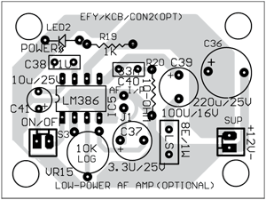
Audio power amplifier

The audio amplifier circuit shown in Fig. 4 is optional. One can use much higher-power audio amplifier along with the audio mixer circuit.

The low-power audio amplifier employing IC LM386 (IC5) shown in Fig. 4 can output a maximum audio power of 1 watt. It gets +12V DC supply at its pin 6. The audio input from sources like Walkman and audio mixer can be fed to pin 3 of IC5 through volume control VR15.

Image may be NSFW.
Clik here to view.
Fig. 3: Power supply circuit

The gain of LM386 is internally set to 20 to keep the external part count low. However, to make LM386 a more versatile amplifier, pins 1 and 8 are provided for setting the gain—externally to any value between 20 and 200—by using an appropriate combination of a resistor and a capacitor. If only a capacitor is put between pins 1 and 8 using switch S3 as shown in Fig. 4, the gain would increase to 200 (46 dB). The amplified output is taken from pin 5 and fed to the loudspeaker through electrolytic capacitor C39 (100 µF). The higher the value of C39, the higher the pitch of the audio frequency response in the speaker.

Image may be NSFW.
Clik here to view.
Fig. 4: Low-power audio amplifier circuit

Power supply. The power supply section for the circuit is shown in Fig. 3. It consists of a step-down transformer (230V AC primary to 12V-0-12V, 1A secondary), bridge rectifier, filter network and regulator ICs 7812 and 7912 to provide +12V and –12V regulated DC outputs, respectively. When switch S1 is closed, the presence of power is indicated by the glowing of LED1.

Construction

Assemble the circuit on any general-purpose PCB. Mount IC bases on the PCB. There is no soldering method that is ideal for all IC packages. The use of IC bases prevents damage to the ICs while soldering and also makes it easy to replace them. Use audio input jack connectors for M1 through M8 input points. Also use audio output connectors at the outputs of IC4.

Image may be NSFW.
Clik here to view.
Fig. 5: Combined actual-size, single-side PCB for audio mixer and power supply circuits
Image may be NSFW.
Clik here to view.
Fig. 6: Components layout for the PCB in Fig. 5

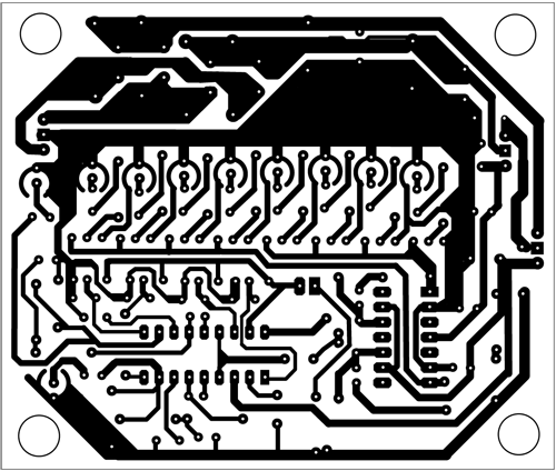
Download PCB and component layout PDFs: click here

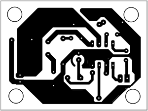
A combined actual-size, single-side PCB layout for Figs 2 and 3 is shown in Fig. 5 and its components layout in Fig. 6. The solder-side PCB layout for Fig. 4 is shown in Fig. 7 and its components layout in Fig. 8.

Note. If you are not using IC base for TDA1524A, the maximum permissible temperature of the solder is 260°C; solder at this temperature must not be in contact with the joint for more than five seconds. The total contact time of successive solder waves must not exceed five seconds while using wave soldering.

Image may be NSFW.
Clik here to view.
Fig. 7: Solder-side PCB layout for the audio amplifier circuit
Image may be NSFW.
Clik here to view.
Fig. 8: Components layout for the PCB in Fig. 7

Testing procedure

  1. After assembling the PCB, check the circuit connections before switching on the power supply.
  2. Use a standard microphone at the first input point M1 and then keep it near an audio source. You can use the power amplifier circuit given here for testing or another higher-output power amplifier.
  3. Vary VR1 slowly until a clear and distortion-free amplified output is obtained.
  4. If the sound output is not clear and VR1 does not help, vary gain control VR9.
  5. If the problem still persists, check volume, balance, bass and treble controls.
  6. Check the various controls in your audio power amplifier section.
  7. Repeat steps 2 through 5 for the rest of the inputs. Having checked all the inputs, now the audio mixer is ready for use.

Feel interested? Check out more circuit projects.

The post Audio Mixer with Multiple Controls appeared first on Electronics For You.


Rechargeable Torch Based on White LED

Image may be NSFW.
Clik here to view.
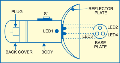
Rechargeable torches don’t come without problems. You need to replace the bulbs and charge the batteries frequently. The average incandescent light-emitting diode (LED) based torch, for instance, consumes around 2 watts. Here’s a white LED based rechargeable torch that consumes just 300 mW and has 60 per cent longer service life than an average incandescent torch.

LED based rechargeable torch circuit

Image may be NSFW.
Clik here to view.
Fig. 1: Circuit diagram of LED based rechargeable torch
Fig. 1: Circuit diagram of the LED based rechargeable torch

Fig. 1 shows the circuit of the rechargeable white LED-based torch. The reactive impedance of capacitors C1 through C3 (rated for 250V AC) limits the current to the charger circuit. The resistor across the capacitors provides a discharge path for the capacitors after the battery is charged. The red LED1 indicates that the circuit is active for charging.

The torch uses three NiMH rechargeable button cells, each of 1.2V, 225 mAH. A normal recharge will take at least 12 hours. Each full recharge will give a continuous operational time of approximately 2.5 hours. Recharge the battery to full capacity immediately after use to ensure its reliability and durability. The charging current is around 25 mA.

Image may be NSFW.
Clik here to view.
Fig. 2: Suggested enclosure for the torch

A voltage booster circuit is required for powering the white LEDs (LED2 through LED4). An inverter circuit is used to achieve voltage boosting. Winding details of the inverter transformer using an insulated ferrite toroidal core is given in the schematic. The number of 35 SWG wire turns in the primary and secondary coils (NP and NS) are 30 and 3, respectively. If the inverter does not oscillate, swap the polarity of either (but not both) the primary or the secondary winding. A reference voltage from resistor R5 provides a reflected biasing to the transistor, and keeps the output constant and regulated.

The suggested enclosure for the torch is shown in Fig. 2.


The post Rechargeable Torch Based on White LED appeared first on Electronics For You.

5V from Portable Wind Turbine

This project deals with the design and development of a portable wind turbine unit, capable of generating electricity from the kinetic energy in the wind. The circuit requires a DC motor, fan blades or propeller, DC-DC boost converter and wind energy to produce a 5V DC output.

Wind-power generation is a fairly simple process that uses an ordinary miniature DC motor to make a very simple wind turbine generator. A miniature DC motor, like RF-300FA-12350, is easily available in the market but can also be taken out from an old CD/DVD drive/player (refer Fig. 1).

Image may be NSFW.
Clik here to view.
Fig. 1: Miniature DC motor
Image may be NSFW.
Clik here to view.
Fig. 2: Wind turbine blades/propeller
Image may be NSFW.
Clik here to view.
Fig. 3: DC-DC boost converter
Image may be NSFW.
Clik here to view.
Fig. 4: Circuit diagram for deriving 5V from the
Fig. 4: Circuit diagram for deriving 5V from the portable wind turbine

A small propeller, or fan blades, can be mounted directly onto the motor shaft. Note that the electricity generated by the motor is DC, and hence no AC-DC conversion circuitry is required apart from a polarity guard diode. In fact, the polarity guard diode is also not required since the propeller rotates in only one direction (counter-clockwise) in this model, due to the unique design structure of the plastic wind turbine blades/propeller.

Compact and light-weight plastic fan blades/propellers are available. A generic three-leg plastic propeller (shown in Fig. 2) is used in this project.

Since a miniature DC motor is used as the rotary engine, only a small amount of DC supply (three to five volts maximum) is available at the output. So, a DC-DC boost converter circuit is required to provide a stable 5V DC output. Any home-made/ready-made DC-DC boost converter circuit can be used for this, however a ready-made DC-DC boost converter module based on pulse frequency modulation (PFM) technique with a standard USB output port, as shown in Fig. 3, is preferred.

If an input voltage of 0.9V to 5V DC is available, this module gives a stable 5V DC output through its USB connector, with conversion efficiency up to 96 percent.

Circuit and working

Image may be NSFW.
Clik here to view.
ZC1_parts
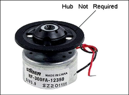
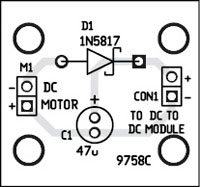
As shown in Fig. 4, the circuit is built around a DC motor, Schottky diode 1N5817 and DC-DC boost converter module. Working of this small DC-DC boost converter module is based on pulse frequency modulation (PFM) technique.

A PFM converter is an alternative DC-DC power converter architecture that uses a variable frequency clock to drive power switches and transfer energy from input to output. Because the drive signal’s frequency is directly controlled to regulate the output voltage, this architecture is referred to as PFM. DC-DC converter with constant-on-time or constant-off-time control is a typical example of this architecture.

In the circuit diagram, the negative terminal (black wire) of DC motor M1 is treated as the positive output terminal, connected to PFM module (board 1) through polarity guard diode 1N5817 (D1), because the motor rotation is in counter-clockwise direction. The PFM module is connected across buffer capacitor (C1) to get a USB-standard 5V DC output through its USB (A-type) connector.

Portable wind turbine construction

An actual-size, single-side PCB for deriving 5V from portable wind turbine is shown in Fig. 5 and its component layout in Fig. 6.

Image may be NSFW.
Clik here to view.
Fig. 5: Actual-size, single-side PCB for deriving 5V from the portable wind turbine
Image may be NSFW.
Clik here to view.
Fig. 6: Component layout of the PCB
Image may be NSFW.
Clik here to view.
Fig. 7: Proposed setup of the portable wind turbine

Download PCB and Component Layout PDFs: Click here

Good air flow is essential for the proper working of the circuit. You can use an ordinary electric fan (or table fan) or an electric air blower as the wind-energy source for testing purpose. Ensure that air flow from the wind source directly falls at the front of the propeller. The propeller should rotate at a fast speed (in counter-clockwise direction) to get higher output.

You need rigid mounting for the wind turbine system. For this, you can fix the motor on a suitable-sized PVC/metal pipe and attach it to a base support as shown in Fig. 7. The base support can be a small-diameter disc made of wood or metal. Connect the PFM module to the circuit at CON1, enclose these in a suitable cabinet and place inside the base in such a way that you can access the USB port conveniently.

Next, route the wires from the DC motor through the pipe to the base and connect the wires to the circuit at M1. Face the propeller towards a wind source. Now, you are ready to get 5V DC output from the USB connector. This output can also be used for charging your mobile phone.

Caution! Rotating blades are sharp and can cause severe injury if not handled properly.


T.K. Hareendran is an electronics hobbyist, freelance technical writer and circuit designer

The post 5V from Portable Wind Turbine appeared first on Electronics For You.

Battery Level Indicator

Normally, in mobile phones, the battery level is shown in dot or bar form. This lets you easily recognise the battery level. Here we present a battery level indicator circuit that lets you know the battery level of a device from the number of LEDs that are glowing. It uses ten LEDs in all. So if three LEDs glow, it indicates battery capacity of 30 per cent.

Unlike in mobile phones where the battery level indicator function is integrated with other functions, here only one comparator IC (LM3914) does it all. The LM3914 uses ten comparators, which are internally assembled in the voltage divider network based on the current-division rule. So it divides the battery level into ten parts.

Battery level indicator circuit

The circuit derives the power supply for its operation from the battery of the device itself. It uses ten LEDs wired in a 10-dot mode. The use of different coloured LEDs makes it easier to recognise the voltage level on the basis of the calibration made. Red LEDs (LED1 through LED3) indicate battery capacity of less than 40 per cent.

Orange LEDs (LED4 through LED6) indicate battery capacity of 40 to less than 70 per cent and green LEDs (LED7 through LED10) indicate battery capacity of 70 to under 100 per cent. The brightness of the LEDs can be adjusted by varying the value of preset VR2 between pins 6 and 7.

Image may be NSFW.
Clik here to view.
Battery Level Indicator Circuit

Diode D1 prevents the circuit from reverse-polarity battery connection. The tenth LED glows only when the battery capacity is full, i.e., the battery is fully charged. When the battery is fully charged, relay-driver transistor T1 conducts to energise relay RL1. This stops the charging through normally-open (N/O) contacts of relay RL1.


For calibration, connect 15V variable, regulated power supply and initially set it at 3V. Slowly adjust VR1 until LED1 glows. Now, increase the input voltage to 15V in steps of 1.

2V until the corresponding LED (LED2 through LED10) lights up.

Now the circuit is ready to show any voltage value with respect to the maximum voltage. As the number of LEDs is ten, we can easily consider one LED for 10 per cent of the maximum voltage.

Construction

Connect the voltage from any battery to be tested at the input probes of the circuit. By examining the number of LEDs glowing you can easily know the status of the battery. Suppose five LEDs are glowing. In this case, the battery capacity is 50 to 59 per cent of its maximum value.

Assemble the circuit on a general-purpose PCB. Calibrate it and then enclose in a box.


Feel interested? check out other electronics projects.

The post Battery Level Indicator appeared first on Electronics For You.

Fuel Reserve Indicator For Vehicles

Image may be NSFW.
Clik here to view.
Here is a simple fuel reserve indicator circuit for monitoring the fuel level in vehicles. It gives an audio-visual indication when the fuel level drops alarmingly below the reserve level, helping you to avoid running out of petrol on the way.

Nowadays vehicles come with a dash-mounted fuel gauge meter that indicates the fuel levels on an analogue display. The ‘reserve’ level is indicated by a red marking in some vehicles, but the needle movement through the red marking may be confusing and not precise. This fuel reserve indicator circuit monitors the fuel tank below the reserve level and warns through LED indicators and audible beeps when the danger level is approaching.

Fuel reserve indicator operation

The fuel reserve indicator circuit system consists of a tank-mounted float sensor and a current meter (fuel meter), which are connected in series. The float-driven sensor attached to an internal rheostat offers high resistance when the tank is empty. When the tank is full, the resistance decreases, allowing more current to pass through the meter to give a higher reading.

The fuel monitoring circuit works by sensing the voltage variation developed across the meter and activates the beeper when the fuel tank is almost empty. Its point A is connected to the input terminal of the fuel meter and point B is connected to the body of the vehicle. The circuit consists of an op-amp IC CA3140 (IC1), two 555 timer ICs (IC2 and IC3) and decade counter CD4017 (IC4).

Circuit operation

Op-amp IC CA3140 is wired as a voltage comparator. Its inverting input (pin 2) receives a reference voltage controlled through VR1. The non-inverting input (pin 3) receives a variable voltage tapped from the input terminal of the fuel meter through resistor R1. When the voltage at pin 3 is higher han at pin 2, the output of IC1 goes high and the green LED (LED1) glows. This condition is maintained until the voltage at pin 3 drops below that at pin 2. When this happens, the output of IC1 swings from high to low, sending a low pulse to the trigger pin of the monostable (usually held high by R3) via C1. The monostable triggers and its output goes high for a predetermined time based on the values of R5 and C2. With the given values, the ‘on’ time will be around four minutes.

The output of IC2 is used to power the astable circuit consisting of timer 555 (IC3) via diode D2. Oscillations of IC3 are controlled by R6, R7, VR2 and C4. With the given values, the ‘on’ and ‘off’ time periods are 27 and 18 seconds, respectively. The pulses from IC3 are given to the clock input (pin 14) of decade counter CD4017 (IC4) and its outputs go high one by one. When the circuit is switched on, LED1 and LED2 glow if your vehicle has sufficient petrol in the tank.

Image may be NSFW.
Clik here to view.
Fuel Reserve Indicator circuit

When the fuel goes below the reserve level, the output of IC1 goes low, LED1 turns off and a negative triggering pulse is received at pin 2 of IC2. The output of IC2 goes high for around four minutes and during this time period, clock pin 14 of IC4 receives the clock pulse (low to high) from the output of IC3.

For the first clock pulse, Q0 output of IC4 goes high and the green LED (LED2) glows for around 50 seconds. On receiving the second clock pulse, Q1 goes high to light up the yellow LED (LED3) and sound the buzzer for around 45 seconds. This audio-visual signal warns you that the vehicle is running out of fuel. On receiving the third clock pulse, LED3 and the buzzer go off. There is a gap of around two-and-a-half minutes before Q5 output goes high.

By the time Q5 goes high and the red LED (LED4) glows, four minutes elapse and the power supply to IC3 is cut off. The output state at Q5 will not change unless a low-to-high clock input is received at its pin 14. Thus LED4 will glow continuously along with the beep. The continuous glowing of the red LED (LED4) and the beep from the buzzer indicate that the vehicle will run out of fuel very shortly.

Q6 output of IC4 is connected to its reset pin 15 via diode D3. This means that after ‘on’ state of Q5, the count will always start from Q0. Capacitor C5 provides power-on reset to IC4 when switch S1 is closed. The output of IC1 is also connected to reset pin of IC4 via diode D1 (1N4148). So when your vehicle is refueled above the reserve level, LED2 glows to indicate that the tank has sufficient fuel.

IC5 provides regulated 12V DC for proper functioning of the circuit even when the battery is charged to more than 12V.

Circuit construction

The circuit can be assembled on a perforated board. Adjust VR1 until the voltage at pin 2 of IC1 drops to 1.5V. When point A is connected to the fuel meter (fuel gauge) terminal that goes to the fuel sensor, green LEDs (LED1 and LED2) glow to indicate the normal fuel level. VR2 can be varied to set the ‘ON’ time period of IC3 at around 20 seconds.

Enclose the circuit in a small case and mount on the dashboard using adhesive tape. The circuit works only in vehicles with negative grounding of the body.

The post Fuel Reserve Indicator For Vehicles appeared first on Electronics For You.

Anti-Sleep Alarm

Image may be NSFW.
Clik here to view.
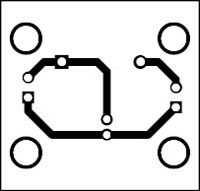
Most of the accidents on highways during night occur due to drivers’ poor vision caused by the continuous exposure of their eyes to the bright light from the headlamps of approaching vehicles. The poor vision is due to exhaustion of the visual pigment in the eyes, which induces sleep to restore the pigment. This anti-sleep alarm keeps you awake.

This circuit keeps you vigilant by sounding intermittent beeps and emitting flashing light so as to remind you that you are not on the bed but driving a vehicle. It works only at night due to the control of a light-dependent resistor (LDR) based switch.

Anti-sleep alarm circuit

The LDR along with two BC548 transistors (T1 and T2) forms the light switch to inhibit the oscillation of IC1 during daytime. As the LDR is exposed to light during daytime, T1 conducts to keep T2 out of conduction. This makes the reset pin (pin 12) of IC1 high to prevent it from oscillation. So the remaining part of the circuit remains in the standby mode.

Image may be NSFW.
Clik here to view.
anti-sleep alarm
Anti-sleep alarm circuit

At night, T1 remains non-conducting as the LDR is in dark. Transistor T2 conducts to pull the reset pin (pin 12) of IC1 to ground. This starts the oscillations of IC1, which is indicated by the flashing of LED1. The internal oscillator of binary counter IC CD4060 oscillates at a frequency based on the values of R5, R6 and C1. Its Q13 output becomes high and low alternately for 15 minutes each. Using potmeter VR1, you can adjust the sensitivity of the LDR.

Circuit operation

When the Q13 output of IC1 becomes high, the reset pin (pin 4) of NE555 astable (IC2) becomes high and it starts oscillating. For the selected values of R10, R11, VR2 and C2, there will be one pulse every 50 seconds. Using VR2, you can slightly adjust the pulse rate. The pulsed output from IC2 is fed to the clock input of IC CD4017 (IC3).

IC CD4017 is a decade counter with ten outputs, but only one of its output is high at a time and all the other outputs remain low. The output from IC2 serves as clock for IC3. As a result, the Q1 output of IC3 becomes high at the first positive edge from IC2 after 50 seconds. After 6 minutes, the Q6 output goes high and LED2 glows for one minute and the warning buzzer sounds.

If the circuit is not reset using push-to-switch S1 after hearing the warning beep from PZ1, the counting of IC3 continues and at the end of the 10th minute, the Q9 output becomes high to activate IC CD4093 (IC4).

Circuit construction

IC4 is wired as a simple oscillator using its two NAND gates 3 and 4. Gate 1 of IC4 is controlled by the status of its input pins 1 and 2. When these pins receive a high output from IC3, the output of gate 1 goes low and the output of gate 2 becomes high. This starts the oscillator built around gates 3 and 4. The frequency of oscillation depends on the values of R13 and C3.

As long as Q9 output of IC3 remains high (i.e., for 15 minutes), IC4 oscillates and the piezobuzzer beeps and the white LEDs flash with a frequency determined by the values of R13 and C3. Thereafter IC4 stops oscillating and the piezobuzzer and the LEDs turn off for another 15 minutes. The cycle repeats every 15 minutes. This is sufficient to alert the napping driver. IC5 and C4 provide regulated 12V DC to the circuit.

The circuit can be constructed on a perforated board and powered from the vehicle’s battery. The assembled unit should be placed in front of the driver seat preferably on the dashboard. Keep LDR1 away from LEDs to allow it to hibernate at night. The power to the circuit should be tapped from the ignition switch so that the circuit functions only when the vehicle is on the road.

The post Anti-Sleep Alarm appeared first on Electronics For You.

Phone Broadcaster

Image may be NSFW.
Clik here to view.
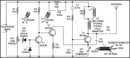
Here is a simple yet very useful phone broadcaster circuit which can be used to eavesdrop on a telephone conversation. The circuit can also be used as a wireless telephone amplifier.

One important feature of this circuit is that the circuit derives its power directly from the active telephone lines, and thus avoids use of any external battery or other power supplies. This not only saves a lot of space but also money. It consumes very low current from telephone lines without disturbing its performance. The circuit is very tiny and can be built using a single-IC type veroboard that can be easily fitted inside a telephone connection box of 3.75 cm x 5 cm.

Phone broadcaster circuit

Image may be NSFW.
Clik here to view.
Phone Broadcaster Circuit

The circuit consists of two sections, namely, automatic switching section and FM transmitter section. Automatic switching section comprises resistors R1 to R3, preset VR1, transistors T1 and T2, zener D2, and diode D1. Resistor R1, along with preset VR1, works as a voltage divider. When voltage across the telephone lines is 48V DC, the voltage available at wiper of preset VR1 ranges from 0 to 32V (adjustable). The switching voltage of the circuit depends on zener breakdown voltage (here 24V) and switching voltage of the transistor T1 (0.7V). Thus, if we adjust preset VR1 to get over 24.7 volts, it will cause the zener to breakdown and transistor T1 to conduct.

As a result collector of transistor T1 will get pulled towards negative supply, to cut off transistor T2. At this stage, if you lift the handset of the telephone, the line voltage drops to about 11V and transistor T1 is cut off. As a result, transistor T2 gets forward biased through resistor R2, to provide a DC path for transistor T3 used in the following FM transmitter section.

The low-power FM transmitter section comprises oscillator transistor T3, coil L1, and a few other components. Transistor T3 works as a common-emitter RF oscillator, with transistor T2 serving as an electronic ‘on’/‘off’ switch. The audio signal available across the telephone lines automatically modulates oscillator frequency via transistor T2 along with itsseries biasing resistor R3. The modulated RF signal is fed to the antenna. The telephone conversation can be heard on an FM receiver remotely when it is tuned to FM transmitter frequency.

Lab Note

During testing of the circuit it was observed that the telephone used was giving an engaged tone when dialed by any subscriber. Addition of resistor R5 and capacitor C6 was found necessary for rectification of the fault.

The post Phone Broadcaster appeared first on Electronics For You.

Decade Counter Based Flash Light

Image may be NSFW.
Clik here to view.
This decade counter based flash light circuit generates flashing lights in running pattern. In conventional running lights, the LEDs glow one by one. In this circuit, the LEDs flash a number of times one by one.

Decade counter based flash light circuit

Image may be NSFW.
Clik here to view.
Decade counter based flash light
Decade counter based flash light circuit

The circuit comprises two astable multivibrators (IC1 and IC3) and a decade counter (IC2). Astable multivibrator IC1 produces approximately 0.72Hz clock frequencies, which are given to decade counter IC2. The decade counter is designed to count Q0, Q1 and Q2 outputs, while its fourth output (Q3) is used to reset it. The Q0, Q1 and Q2 outputs of IC2 are fed to npn transistors T1, T2 and T3, respectively. The collectors of transistors T1, T2 and T3 are connected to the emitter of transistor T4, while their emitters are connected to LED1, LED2 and LED3 via 150-ohm resistors R6, R7 and R8, respectively.The LEDs are activated one by one by the decade counter outputs.

Astable multivibrator IC3 produces approximately 8.4Hz clock, which is given to transistor T4 via resistor R9 to switch on the supply to transistors T1 through T3 for each positive half cycle of IC3 output.

Now for each output period of IC2, a particular LED blinks at the rate of 8.4 Hz. The blinking then shifts to the next LED when the output of IC2 advances by one count (after about 1.3 seconds). Similarly, the blinking effect shifts to the next LED after another 1.3 seconds and the cycle repeats thereafter.

Flashing frequencies can be changed by changing the values of R10 and R11 and capacitor C4. The circuit can be easily assembled on any general-purpose PCB. It works off a 12V regulated power supply. You can also add more LEDs in series with LED1, LED2 and LED3, respectively.

The post Decade Counter Based Flash Light appeared first on Electronics For You.


Viewing all 48 articles
Browse latest View live